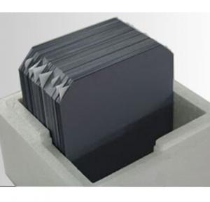


Solar Mono Silicon Wafer for Solar Cell (156 and 125)
- Ref Price:
-

- Loading Port:
- China main port
- Payment Terms:
- TT or LC
- Min Order Qty:
- 10000 pc
- Supply Capability:
- 1000000 pc/month
OKorder Service Pledge
OKorder Financial Service
You Might Also Like


1. Structure of Solar Mono Silicon Wafer for Solar Cell (156 and 125) Description
A wafer, also called a slice or substrate, is a thin slice of semiconductor material, such as acrystalline silicon, used in electronics for the
fabrication of integrated circuits and in photovoltaics for conventional, wafer-based solar cells. The wafer serves as the substrate for
microelectronic devices built in and over the wafer and undergoes many microfabrication process steps such as doping or ion
implantation,etching, deposition of various materials, and photolithographic patterning. Finally the individual microcircuits are separated
(dicing) and packaged.
2. Main Features of the Solar Mono Silicon Wafer for Solar Cell (156 and 125)
• High quality Silicon wafer carrier box
• quartz glass wafer carrier from Taifulong Technology
3. Solar Mono Silicon Wafer for Solar Cell (156 and 125) Images
")
")
4. Solar Mono Silicon Wafer for Solar Cell (156 and 125) Specification
窗体顶端 Item窗体底端 | N-type solar grade mono silicon wafer(125x125mm) | N-type solar grade mono silicon wafer(156x156mm) |
Growth Method | CZ | CZ |
Conductive Type | N-type | N-type |
Dopant | Phos. | Phos. |
Orientation | <100>±3° | <100>±3° |
Resistivity | 1 –3,3-6Ω•cm | 1 –3,3-6 Ω•cm |
Bulk Lifetime | ≥1000μs | ≥1000μs |
Oxygen Content | ≤0.1*1018 cm3 | ≤0.1*1018 cm3 |
Carbon Content | ≤0.1*1017 /cm3 | ≤0.1*1017 /cm3 |
Dimension | 125*125±0.5mm | 156*156±0.5mm |
Diagonal | 150±0.5mm | 200±0.5mm |
Square Sides Angle | 90±0.3° | 90±0.3° |
Thickness | 200±20 um | 200±20 um |
TTV | ≤25um | ≤25um |
Saw Mark | ≤15um | ≤15um |
Warp | ≤40um | ≤40um |
Chips | Depth<0.3mm;Length<0.5mm | Depth<0.3mm;Length<0.5mm, |
less than 2chips per wafer | less than 2chips per wafer | |
Appearance | No Stain, No Pinhole and Cracks by Visual Inspection | No Stain, No Pinhole and Cracks by Visual Inspection |
Dislocation Density | ≤1000 pcs/cm2 | ≤1000 pcs/cm2 |
Package | Packed in Polyethylene foam box,400pcs/box | Packed in Polyethylene foam box,400pcs/box 窗体底端 |
5. FAQ of Solar Mono Silicon Wafer for Solar Cell (156 and 125)
Q1. How long can we receive the product after purchase?
A1.In the purchase of product within three working days, We will arrange the factory delivery as soon as possible. The pecific time of receiving is related to the state and position of customers
Q2. Can we visit your factory?
A2:Surely, I will arrange the trip basing on your business schedule.
Q3:Which payment terms can you accept?
A3:T/T,L/C,Moneygram,Paypal are available for us.
- Q:Are solar silicon wafers affected by power fluctuations?
- Yes, solar silicon wafers can be affected by power fluctuations. Fluctuations in power supply can impact the efficiency and performance of solar panels, including the silicon wafers used in their construction. Such fluctuations can potentially lead to reduced power output or even damage the panels if not adequately managed or protected.
- Q:Can solar silicon wafers be used in solar-powered water pumps?
- Yes, solar silicon wafers can be used in solar-powered water pumps. The wafers are used to convert sunlight into electricity, which can then be used to power the water pump.
- Q:How are solar silicon wafers protected from electrical surges?
- Solar silicon wafers are protected from electrical surges through the use of protective devices called surge protectors or transient voltage suppressors. These devices are connected in parallel to the solar panels and have the capability to divert excess voltage or current away from the wafers during sudden electrical surges. This helps prevent damage to the wafers and ensures the longevity and efficiency of the solar panels.
- Q:How do solar silicon wafers perform in cold climates?
- Solar silicon wafers perform well in cold climates as the low temperatures actually enhance their efficiency. The cold weather helps to reduce the resistance in the solar cells, allowing them to produce more electricity. However, extreme cold can lead to issues such as snow accumulation, which may temporarily hinder their performance until cleared. Overall, solar silicon wafers are designed to withstand and operate efficiently in cold weather conditions.
- Q:Can solar silicon wafers be used in solar-powered security systems?
- Yes, solar silicon wafers can be used in solar-powered security systems. These wafers are commonly used to create solar panels that generate electricity from sunlight. By utilizing solar silicon wafers in solar-powered security systems, the systems can operate independently from the electrical grid, making them more versatile and efficient.
- Q:Are there any environmental concerns with the production or disposal of solar silicon wafers?
- Yes, there are some environmental concerns associated with the production and disposal of solar silicon wafers. The production process of silicon wafers requires significant energy consumption and can contribute to carbon emissions if the energy source used is not renewable. Additionally, the extraction of raw materials, such as quartz, for silicon production can have negative environmental impacts. In terms of disposal, while silicon wafers are not typically hazardous waste, improper disposal can still contribute to electronic waste accumulation and pose potential risks if not managed properly. However, it is important to note that compared to other forms of energy production, the overall environmental impact of solar silicon wafer production and disposal is still relatively low.
- Q:How thick are solar silicon wafers?
- Solar silicon wafers typically have a thickness ranging from 150 to 200 micrometers (μm), which is about 0.15 to 0.2 millimeters (mm).
- Q:How do solar silicon wafers compare to other types of solar cell technologies?
- Solar silicon wafers, commonly used in crystalline silicon solar cells, have several advantages over other types of solar cell technologies. Firstly, they have high efficiency levels, with conversion rates reaching up to 25%. Additionally, silicon wafers are well-established and have a long track record of reliability and durability. They are also readily available and affordable due to mass production. However, silicon wafers require a significant amount of energy and resources during manufacturing. In contrast, other solar cell technologies like thin-film solar cells may have lower efficiency but offer flexibility, lighter weight, and lower manufacturing costs. Ultimately, the choice between solar silicon wafers and other technologies depends on specific requirements such as cost, efficiency, and application.
- Q:Are there any alternatives to using solar silicon wafers in solar cells?
- Yes, there are several alternatives to using solar silicon wafers in solar cells. Some of these alternatives include thin-film solar cells made from materials such as cadmium telluride (CdTe), copper indium gallium selenide (CIGS), and organic photovoltaic materials. These alternative materials offer advantages such as lower manufacturing costs, flexibility, and higher energy conversion efficiencies. However, each alternative has its own set of limitations and challenges that need to be addressed for widespread adoption.
- Q:Are solar silicon wafers affected by voltage fluctuations?
- Yes, solar silicon wafers can be affected by voltage fluctuations. Voltage fluctuations can impact the overall performance and efficiency of solar panels, potentially leading to reduced power output. It is important to maintain a stable and consistent voltage supply to optimize the performance and lifespan of solar silicon wafers.
1. Manufacturer Overview |
|
|---|---|
| Location | |
| Year Established | |
| Annual Output Value | |
| Main Markets | |
| Company Certifications | |
2. Manufacturer Certificates |
|
|---|---|
| a) Certification Name | |
| Range | |
| Reference | |
| Validity Period | |
3. Manufacturer Capability |
|
|---|---|
| a)Trade Capacity | |
| Nearest Port | |
| Export Percentage | |
| No.of Employees in Trade Department | |
| Language Spoken: | |
| b)Factory Information | |
| Factory Size: | |
| No. of Production Lines | |
| Contract Manufacturing | |
| Product Price Range | |
Send your message to us
Solar Mono Silicon Wafer for Solar Cell (156 and 125)
- Ref Price:
-
- Loading Port:
- China main port
- Payment Terms:
- TT or LC
- Min Order Qty:
- 10000 pc
- Supply Capability:
- 1000000 pc/month
OKorder Service Pledge
OKorder Financial Service
Similar products


New products
Hot products


Hot Searches
Related keywords