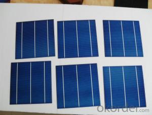


High Current Solar Cell 17.0% Polycrystalline Silicon Solar Cell Price
- Ref Price:
-

- Loading Port:
- Shanghai
- Payment Terms:
- TT OR LC
- Min Order Qty:
- 1000 pc
- Supply Capability:
- 100000 pc/month
OKorder Service Pledge
OKorder Financial Service
You Might Also Like


4 Bus Bars 156*156 17.6% efficiency poly solar cell
PHYSICAL CHARACTERISTICS
Dimension: 156mm x 156mm ± 0.5mm
Wafer Thickeness: 180um+20um and 200um+20um
Front(-) Four 1.2mm silver busbar
Silicon nitride blue anti-reflection coating
Back(+) aluminum back surface field
1.75mm(silver) wide segment soldering pads

Typical Electrical Characteristics
Efficiency | W(Pmpp) | V(Umpp) | A(Impp) | V(Uoc) | A(Isc) |
17.4-17.5 | 4.234 | 0.517 | 8.231 | 0.622 | 8.759 |
17.5-17.6 | 4.259 | 0.519 | 8.243 | 0.623 | 8.769 |
17.7-17.8 | 4.283 | 0.521 | 8.256 | 0.625 | 8.779 |
17.8-17.9 | 4.307 | 0.523 | 8.268 | 0.626 | 8.788 |
17.9-18.0 | 4.332 | 0.525 | 8.281 | 0.627 | 8.798 |
18.0-18.1 | 4.380 | 0.529 | 8.306 | 0.629 | 8.808 |
18.1-18.2 | 4.405 | 0.531 | 8.318 | 0.632 | 8.818 |
18.2-18.3 | 4.429 | 0.533 | 8.331 | 0.633 | 8.837 |
18.3-18.4 | 4.453 | 0.535 | 8.344 | 0.634 | 8.847 |
18.4-18.5 | 4.478 | 0.537 | 8.356 | 0.636 | 8.856 |
18.5-18.6 | 4.502 | 0.539 | 8.369 | 0.637 | 8.866 |
Efficiency | W(Pmpp) | V(Umpp) | A(Impp) | V(Uoc) | A(Isc) |
20.90-21.00 | 5.06 | 0.557 | 9.007 | 0.653 | 9.688 |
20.80-20.90 | 5.04 | 0.556 | 9.062 | 0.652 | 9.683 |
20.70-20.80 | 5.02 | 0.554 | 9.055 | 0.651 | 9.684 |
20.60-20.70 | 4.99 | 0.552 | 9.033 | 0.651 | 9.672 |
20.50-20.60 | 4.97 | 0.550 | 9.002 | 0.650 | 9.673 |
20.40-20.50 | 4.94 | 0.548 | 9.012 | 0.649 | 9.674 |
20.30-20.40 | 4.92 | 0.546 | 9.009 | 0.649 | 9.655 |
20.20-20.30 | 4.89 | 0.543 | 9.012 | 0.648 | 9.634 |
20.10-20.20 | 4.87 | 0.541 | 8.998 | 0.648 | 9.617 |
20.00-20.10 | 4.85 | 0.540 | 8.977 | 0.647 | 9.600 |
*Data under standard testing conditional (STC):1,000w/m2,AM1.5, 25°C , Pmax:Positive power tolerance.
3 Bus Bars 156*156 17.4% efficiency poly solar cell
Dimension: 156 mm x 156 mm ± 0.5 mm
Wafer Thickeness: 156 mm x 156 mm ± 0.5 mm

Typical Electrical Characteristics:
| Efficiency code | 1660 | 1680 | 1700 | 1720 | 1740 | 1760 | 1780 | 1800 | 1820 | 1840 | 1860 |
| Efficiency (%) | 16.6 | 16.8 | 17.0 | 17.2 | 17.4 | 17.6 | 17.8 | 18.0 | 18.2 | 18.4 | 18.6 |
| Pmax (W) | 4.04 | 4.09 | 4.14 | 4.19 | 4.23 | 4.28 | 4.33 | 4.38 | 4.43 | 4.48 | 4.53 |
| Voc (V) | 0.612 | 0.615 | 0.618 | 0.621 | 0.624 | 0.627 | 0.629 | 0.63 | 0.633 | 0.635 | 0.637 |
| Isc (A) | 8.42 | 8.46 | 8.51 | 8.56 | 8.61 | 8.65 | 8.69 | 8.73 | 8.77 | 8.81 | 8.84 |
| Imp (A) | 7.91 | 7.99 | 8.08 | 8.16 | 8.22 | 8.27 | 8.33 | 8.38 | 8.43 | 8.48 | 8.53 |
* Testing conditions: 1000 W/m2, AM 1.5, 25 °C, Tolerance: Efficiency ± 0.2% abs., Pmpp ±1.5% rel.
* Imin : at 0.5 V
Production:

Package:

FAQ:
1. Q: Do you have your own factory?
A: Yes, we have. Our factory located in Jiangsu
2. Q: How can I visit your factory?
A: Before you visit,please contact us.We will show you the route or arrange a car to pick you up.
3. Q: Do you provide free sample?
A: Commenly we provide paid sample.
4. Q: Could you print our company LOGO on the nameplate and package?
A: Yes, we accept it.And need an Authorization Letter from you.
5. Q: Do you accept custom design on size?
A: Yes, if the size is reasonable.
6. Q: How can I be your agent in my country?
A: Please leave feedback. It's better for us to talk about details by email.
7. Q: Do you have solar project engineer who can guide me to install system?
A: Yes, we have a professional engineer team. They can teach you how to install a solar system.
- Q:Can solar silicon wafers be used in concentrated solar power (CSP) systems?
- Yes, solar silicon wafers can be used in concentrated solar power (CSP) systems. CSP systems use mirrors or lenses to concentrate sunlight onto a receiver, which then converts the solar energy into thermal or electrical energy. Silicon wafers can be used as the receiver material in CSP systems to efficiently capture and convert the concentrated sunlight into electricity.
- Q:I would like to ask: silicon annealing treatment is how? Why anneal? Does annealing have an effect on the resistivity and the minority lifetime?
- Another fact: if the same "complement", can be understood as: oxygen from the surface after the removal of impurities, near the surface of the reduced defects is also reduced, the mean free path of carrier mobility increases, also increases, which leads to the decrease of resistivity.
- Q:What is the role of the front contact on a solar silicon wafer?
- The front contact on a solar silicon wafer plays a crucial role in the conversion of sunlight into electricity. It acts as a conductive layer that collects the electrical current generated by the solar cells. Additionally, the front contact helps in reflecting and trapping sunlight, allowing for better absorption and utilization of solar energy. It also protects the underlying layers of the solar cell from external factors such as moisture, dust, and corrosion, thereby ensuring the longevity and efficiency of the solar panel.
- Q:Can solar silicon wafers be used in solar-powered street lighting?
- Yes, solar silicon wafers can be used in solar-powered street lighting. These wafers are commonly used in solar panels to convert sunlight into electricity, which can then be used to power various applications, including street lighting systems. Solar-powered street lights harness the energy from the sun through the silicon wafers, allowing them to operate independently from the electrical grid, making them environmentally friendly and cost-effective.
- Q:How are solar silicon wafers protected from chemical damage?
- Solar silicon wafers are protected from chemical damage through the application of various protective layers. These layers act as barriers between the wafer and potentially harmful chemicals, preventing them from corroding or contaminating the silicon surface. Additionally, the wafers are often covered with anti-reflective coatings that not only enhance their efficiency but also provide an extra level of protection against chemical exposure.
- Q:How are solar silicon wafers affected by potential-induced degradation?
- Solar silicon wafers are negatively affected by potential-induced degradation (PID). PID occurs when high voltage potential differences between the solar cells and their grounded frames cause leakage currents to flow through the silicon wafers. This leads to a decrease in the power output and efficiency of the solar panels over time. PID can significantly impact the performance and lifespan of solar photovoltaic systems, making it crucial to implement preventive measures and use PID-resistant materials and designs to mitigate its effects.
- Q:How long do solar silicon wafers last?
- Solar silicon wafers have a long lifespan and can last for several decades. With proper maintenance and care, they can continue to generate electricity efficiently for at least 25 to 30 years.
- Q:What is the role of metal contacts on solar silicon wafers?
- The role of metal contacts on solar silicon wafers is to provide electrical connections between the solar cells and external devices, such as wires or other components in the solar panel system. These contacts help to efficiently extract the generated electricity from the solar cells and transfer it to the desired output.
- Q:What are the advantages of using a solar silicon wafer?
- One of the main advantages of using a solar silicon wafer is its high efficiency in converting sunlight into electricity. Silicon wafers have excellent electrical properties and can absorb a wide range of solar wavelengths, maximizing energy conversion. Additionally, silicon is abundant and readily available, making it a cost-effective option for solar panel manufacturing. Furthermore, silicon wafers are durable and have a long lifespan, ensuring reliable power generation for many years.
- Q:Can solar silicon wafers be used in all types of solar panels?
- Yes, solar silicon wafers can be used in all types of solar panels. Silicon is the most commonly used material in solar cells, and it can be processed into different types of wafers to suit various panel designs and technologies, including monocrystalline, polycrystalline, and thin-film solar panels.
1. Manufacturer Overview |
|
|---|---|
| Location | |
| Year Established | |
| Annual Output Value | |
| Main Markets | |
| Company Certifications | |
2. Manufacturer Certificates |
|
|---|---|
| a) Certification Name | |
| Range | |
| Reference | |
| Validity Period | |
3. Manufacturer Capability |
|
|---|---|
| a)Trade Capacity | |
| Nearest Port | |
| Export Percentage | |
| No.of Employees in Trade Department | |
| Language Spoken: | |
| b)Factory Information | |
| Factory Size: | |
| No. of Production Lines | |
| Contract Manufacturing | |
| Product Price Range | |
Send your message to us
High Current Solar Cell 17.0% Polycrystalline Silicon Solar Cell Price
- Ref Price:
-
- Loading Port:
- Shanghai
- Payment Terms:
- TT OR LC
- Min Order Qty:
- 1000 pc
- Supply Capability:
- 100000 pc/month
OKorder Service Pledge
OKorder Financial Service
Similar products


New products
Hot products


Hot Searches
Related keywords