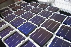


High Current Solar Cell 16.6% Polycrystalline Silicon Solar Cell Price
- Ref Price:
-

- Loading Port:
- Shanghai
- Payment Terms:
- TT OR LC
- Min Order Qty:
- 1000 pc
- Supply Capability:
- 100000 pc/month
OKorder Service Pledge
OKorder Financial Service
You Might Also Like


4 Bus Bars 156*156 17.6% efficiency poly solar cell
PHYSICAL CHARACTERISTICS
Dimension: 156mm x 156mm ± 0.5mm
Wafer Thickeness: 180um+20um and 200um+20um
Front(-) Four 1.2mm silver busbar
Silicon nitride blue anti-reflection coating
Back(+) aluminum back surface field
1.75mm(silver) wide segment soldering pads

Typical Electrical Characteristics
Efficiency | W(Pmpp) | V(Umpp) | A(Impp) | V(Uoc) | A(Isc) |
17.4-17.5 | 4.234 | 0.517 | 8.231 | 0.622 | 8.759 |
17.5-17.6 | 4.259 | 0.519 | 8.243 | 0.623 | 8.769 |
17.7-17.8 | 4.283 | 0.521 | 8.256 | 0.625 | 8.779 |
17.8-17.9 | 4.307 | 0.523 | 8.268 | 0.626 | 8.788 |
17.9-18.0 | 4.332 | 0.525 | 8.281 | 0.627 | 8.798 |
18.0-18.1 | 4.380 | 0.529 | 8.306 | 0.629 | 8.808 |
18.1-18.2 | 4.405 | 0.531 | 8.318 | 0.632 | 8.818 |
18.2-18.3 | 4.429 | 0.533 | 8.331 | 0.633 | 8.837 |
18.3-18.4 | 4.453 | 0.535 | 8.344 | 0.634 | 8.847 |
18.4-18.5 | 4.478 | 0.537 | 8.356 | 0.636 | 8.856 |
18.5-18.6 | 4.502 | 0.539 | 8.369 | 0.637 | 8.866 |
Efficiency | W(Pmpp) | V(Umpp) | A(Impp) | V(Uoc) | A(Isc) |
20.90-21.00 | 5.06 | 0.557 | 9.007 | 0.653 | 9.688 |
20.80-20.90 | 5.04 | 0.556 | 9.062 | 0.652 | 9.683 |
20.70-20.80 | 5.02 | 0.554 | 9.055 | 0.651 | 9.684 |
20.60-20.70 | 4.99 | 0.552 | 9.033 | 0.651 | 9.672 |
20.50-20.60 | 4.97 | 0.550 | 9.002 | 0.650 | 9.673 |
20.40-20.50 | 4.94 | 0.548 | 9.012 | 0.649 | 9.674 |
20.30-20.40 | 4.92 | 0.546 | 9.009 | 0.649 | 9.655 |
20.20-20.30 | 4.89 | 0.543 | 9.012 | 0.648 | 9.634 |
20.10-20.20 | 4.87 | 0.541 | 8.998 | 0.648 | 9.617 |
20.00-20.10 | 4.85 | 0.540 | 8.977 | 0.647 | 9.600 |
*Data under standard testing conditional (STC):1,000w/m2,AM1.5, 25°C , Pmax:Positive power tolerance.
3 Bus Bars 156*156 17.4% efficiency poly solar cell
Dimension: 156 mm x 156 mm ± 0.5 mm
Wafer Thickeness: 156 mm x 156 mm ± 0.5 mm

Typical Electrical Characteristics:
| Efficiency code | 1660 | 1680 | 1700 | 1720 | 1740 | 1760 | 1780 | 1800 | 1820 | 1840 | 1860 |
| Efficiency (%) | 16.6 | 16.8 | 17.0 | 17.2 | 17.4 | 17.6 | 17.8 | 18.0 | 18.2 | 18.4 | 18.6 |
| Pmax (W) | 4.04 | 4.09 | 4.14 | 4.19 | 4.23 | 4.28 | 4.33 | 4.38 | 4.43 | 4.48 | 4.53 |
| Voc (V) | 0.612 | 0.615 | 0.618 | 0.621 | 0.624 | 0.627 | 0.629 | 0.63 | 0.633 | 0.635 | 0.637 |
| Isc (A) | 8.42 | 8.46 | 8.51 | 8.56 | 8.61 | 8.65 | 8.69 | 8.73 | 8.77 | 8.81 | 8.84 |
| Imp (A) | 7.91 | 7.99 | 8.08 | 8.16 | 8.22 | 8.27 | 8.33 | 8.38 | 8.43 | 8.48 | 8.53 |
* Testing conditions: 1000 W/m2, AM 1.5, 25 °C, Tolerance: Efficiency ± 0.2% abs., Pmpp ±1.5% rel.
* Imin : at 0.5 V
Production:

Package:

FAQ:
1. Q: Do you have your own factory?
A: Yes, we have. Our factory located in Jiangsu
2. Q: How can I visit your factory?
A: Before you visit,please contact us.We will show you the route or arrange a car to pick you up.
3. Q: Do you provide free sample?
A: Commenly we provide paid sample.
4. Q: Could you print our company LOGO on the nameplate and package?
A: Yes, we accept it.And need an Authorization Letter from you.
5. Q: Do you accept custom design on size?
A: Yes, if the size is reasonable.
6. Q: How can I be your agent in my country?
A: Please leave feedback. It's better for us to talk about details by email.
7. Q: Do you have solar project engineer who can guide me to install system?
A: Yes, we have a professional engineer team. They can teach you how to install a solar system.
- Q:Can solar silicon wafers be used in military applications?
- Yes, solar silicon wafers can be used in military applications. They can be integrated into various military technologies such as portable power systems, surveillance equipment, and remote communication devices to provide a reliable and sustainable source of energy in the field.
- Q:What is the expected efficiency improvement for tandem perovskite-silicon solar silicon wafers?
- The expected efficiency improvement for tandem perovskite-silicon solar silicon wafers is significant, potentially reaching beyond 30%.
- Q:How does the crystal structure of a solar silicon wafer affect its performance?
- The crystal structure of a solar silicon wafer plays a crucial role in determining its performance. The wafer's crystal structure affects its electrical properties, such as conductivity and efficiency, which directly impact the efficiency of solar cells made from these wafers. A well-aligned crystal structure with minimal defects allows for better electron flow and reduces recombination losses, resulting in higher conversion efficiency. Additionally, a uniform crystal structure ensures consistent performance across the entire wafer, maximizing the overall energy output of the solar cell.
- Q:Can solar silicon wafers be used in floating solar panel installations?
- Yes, solar silicon wafers can be used in floating solar panel installations. These wafers are commonly used in traditional solar panel systems and can also be adapted for floating installations. The key difference lies in the mounting structure and anchoring mechanisms, which are designed to keep the panels afloat on bodies of water.
- Q:What is the impact of stress and strain on solar silicon wafers?
- The impact of stress and strain on solar silicon wafers can be detrimental to their performance and overall efficiency. Excessive stress and strain can lead to the formation of defects and cracks in the wafers, which can impair their electrical conductivity and structural integrity. These defects can reduce the conversion efficiency of solar cells and increase the likelihood of failure over time. Therefore, it is crucial to carefully manage stress and strain during the manufacturing and handling processes to ensure the optimal performance and longevity of solar silicon wafers.
- Q:Can solar silicon wafers be used in off-grid lighting systems?
- Yes, solar silicon wafers can be used in off-grid lighting systems. These wafers are essential components of solar panels, which convert sunlight into electricity. In off-grid lighting systems, solar panels with silicon wafers collect energy from the sun during the day, store it in batteries, and then power the lighting system during the night. This allows for sustainable and environmentally friendly lighting solutions in areas without access to electricity grids.
- Q:How do solar silicon wafers perform in high rainfall regions?
- Solar silicon wafers perform well in high rainfall regions as rainwater helps in cleaning the surface, resulting in improved efficiency and performance. Additionally, the smooth surface of silicon wafers prevents water from accumulating, reducing the risk of damage or short-circuiting. However, it is important to note that regular maintenance and cleaning might be required to ensure optimal performance in such regions.
- Q:How are solar silicon wafers cut from a silicon ingot?
- Solar silicon wafers are typically cut from a silicon ingot using a process called wire sawing. In this method, a wire made of a hard and abrasive material, such as diamond, is used to slice through the ingot. The wire is guided by a set of pulleys and continuously fed with a slurry mixture of silicon carbide and water to aid in the cutting process. As the wire moves through the ingot, it gradually separates it into thin wafers, which can then be further processed and used in the production of solar cells.
- Q:Can solar silicon wafers be used in solar-powered desalination systems?
- Yes, solar silicon wafers can be used in solar-powered desalination systems. These wafers are commonly used to produce solar cells, which convert sunlight into electricity. By integrating solar silicon wafers into the desalination system, the generated electricity can power the process of removing salt and impurities from seawater, making it suitable for drinking or irrigation purposes.
- Q:How is a solar silicon wafer cut?
- A solar silicon wafer is typically cut using a process called wire sawing. In this method, a diamond-coated wire is used to slowly cut through the silicon ingot, creating thin slices of silicon wafers. This technique allows for precise and efficient cutting, resulting in high-quality solar cells.
1. Manufacturer Overview |
|
|---|---|
| Location | |
| Year Established | |
| Annual Output Value | |
| Main Markets | |
| Company Certifications | |
2. Manufacturer Certificates |
|
|---|---|
| a) Certification Name | |
| Range | |
| Reference | |
| Validity Period | |
3. Manufacturer Capability |
|
|---|---|
| a)Trade Capacity | |
| Nearest Port | |
| Export Percentage | |
| No.of Employees in Trade Department | |
| Language Spoken: | |
| b)Factory Information | |
| Factory Size: | |
| No. of Production Lines | |
| Contract Manufacturing | |
| Product Price Range | |
Send your message to us
High Current Solar Cell 16.6% Polycrystalline Silicon Solar Cell Price
- Ref Price:
-
- Loading Port:
- Shanghai
- Payment Terms:
- TT OR LC
- Min Order Qty:
- 1000 pc
- Supply Capability:
- 100000 pc/month
OKorder Service Pledge
OKorder Financial Service
Similar products


New products

Hot products


Hot Searches
Related keywords