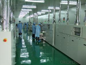
Solar Cell High Quality A Grade Cell Polyrystalline 5v 16.0%
- Ref Price:
-

- Loading Port:
- Shanghai
- Payment Terms:
- TT OR LC
- Min Order Qty:
- 1000 pc
- Supply Capability:
- 100000 pc/month
OKorder Service Pledge
OKorder Financial Service
You Might Also Like


Specifications
hot sale solar cell
1.16.8%~18.25% high efficiency
2.100% checked quality
3.ISO9001/ISO14001/TUV/CE/UL
4.stable performance
We can offer you the best quality products and services, don't miss !
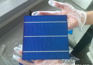
POLY6'(156*156)
Polycrystalline Silicon Solar cell
Physical Characteristics
Dimension: 156mm×156mm±0.5mm
Diagonal: 220mm±0.5mm
Thickness(Si): 200±20 μm
Front(-) Back(+)
Blue anti-reflecting coating (silicon nitride); Aluminum back surface field;
1.5mm wide bus bars; 2.0mm wide soldering pads;
Distance between bus bars: 51mm . Distance between bus bars :51mm .
Electrical Characteristics
Efficiency(%) | 18.00 | 17.80 | 17.60 | 17.40 | 17.20 | 16.80 | 16.60 | 16.40 | 16.20 | 16.00 | 15.80 | 15.60 |
Pmpp(W) | 4.33 | 4.29 | 4.24 | 4.19 | 4.14 | 4.09 | 4.04 | 3.99 | 3.94 | 3.90 | 3.86 | 3.82 |
Umpp(V) | 0.530 | 0.527 | 0.524 | 0.521 | 0.518 | 0.516 | 0.514 | 0.511 | 0.509 | 0.506 | 0.503 | 0.501 |
Impp(A) | 8.159 | 8.126 | 8.081 | 8.035 | 7.990 | 7.938 | 7.876 | 7.813 | 7.754 | 7.698 | 7.642 | 7.586 |
Uoc(V) | 0.633 | 0.631 | 0.628 | 0.625 | 0.623 | 0.620 | 0.618 | 0.617 | 0.615 | 0.613 | 0.611 | 0.609 |
Isc(A) | 8.709 | 8.677 | 8.629 | 8.578 | 8.531 | 8.478 | 8.419 | 8.356 | 8.289 | 8.220 | 8.151 | 8.083 |

MONO5'(125*125mm)165
Monocrystalline silicon solar cell
Physical Characteristics
Dimension: 125mm×125mm±0.5mm
Diagonal: 165mm±0.5mm
Thickness(Si): 200±20 μm
Front(-) Back(+)
Blue anti-reflecting coating(silicon nitride); Aluminum back surface field;
1.6mmwide bus bars; 2.5mm wide soldering pads;
Distance between bus bars: 61mm . Distance between bus bars :61mm .
Electrical Characteristics
Efficiency(%) | 19.40 | 19.20 | 19.00 | 18.80 | 18.60 | 18.40 | 18.20 | 18.00 | 17.80 | 17.60 | 17.40 | 17.20 |
Pmpp(W) | 2.97 | 2.94 | 2.91 | 2.88 | 2.85 | 2.82 | 2.79 | 2.76 | 2.73 | 2.70 | 2.67 | 2.62 |
Umpp(V) | 0.537 | 0.535 | 0.533 | 0.531 | 0.527 | 0.524 | 0.521 | 0.518 | 0.516 | 0.515 | 0.513 | 0.509 |
Impp(A) | 5.531 | 5.495 | 5.460 | 5.424 | 5.408 | 5.382 | 5.355 | 5.328 | 5.291 | 5.243 | 5.195 | 4.147 |
Uoc(V) | 0.637 | 0.637 | 0.636 | 0.635 | 0.633 | 0.630 | 0.629 | 0.629 | 0.628 | 0.626 | 0.626 | 0.625 |
Isc(A) | 5.888 | 5.876 | 5.862 | 5.848 | 5.839 | 5.826 | 5.809 | 5.791 | 5.779 | 5.756 | 5.293 | 5.144 |

FAQ:
Q:How can i get some sample?
A:Yes , if you want order ,sample is not a problem.
Q:How about your solar panel efficency?
A: Our product efficency around 17.25%~18.25%.
Q:What’s the certificate you have got?
A: we have overall product certificate of ISO9001/ISO14001/CE/TUV/UL
- Q:What is the role of surface passivation layers on solar silicon wafers?
- The role of surface passivation layers on solar silicon wafers is to minimize surface recombination, which significantly improves the efficiency of solar cells. These layers act as a barrier, preventing the loss of charge carriers and reducing the chances of electron-hole pairs recombining at the surface. By passivating the surface, these layers help to enhance the electrical properties of the solar cell, allowing for better absorption and conversion of sunlight into electricity.
- Q:Can solar silicon wafers be used in aerospace applications?
- Yes, solar silicon wafers can be used in aerospace applications. They are commonly utilized in the construction of solar panels for spacecraft and satellites to harness solar energy for power generation in space.
- Q:Why integrated circuits are rectangular and the silicon chips are round
- Chip makers use a number of processes to integrate the integrated circuit on the circle. And an integrated circuit with more than a dozen or even hundreds of chips. After the completion of the results according to India to cut it, cut into small pieces of a small square. Then the small silicon chip is packaged with other materials and pins into an integrated circuit chip.
- Q:How does the efficiency of a solar silicon wafer change with shade?
- The efficiency of a solar silicon wafer decreases significantly when it is shaded. Shade interrupts the flow of sunlight onto the wafer's surface, which reduces the amount of solar energy that can be converted into electricity. Even a small amount of shade can have a noticeable impact on its performance, leading to a decrease in overall efficiency.
- Q:How does surface roughness affect the efficiency of a solar silicon wafer?
- Surface roughness affects the efficiency of a solar silicon wafer by influencing the amount of light that is absorbed and reflected. A smoother surface allows for more light to be absorbed into the wafer, increasing its efficiency. Conversely, a rougher surface scatters and reflects more light, reducing the overall efficiency of the solar cell.
- Q:Can solar silicon wafers be used in solar-powered space vehicles?
- Yes, solar silicon wafers can be used in solar-powered space vehicles. These wafers are commonly used in the production of solar panels, which are essential for capturing solar energy in space. The high efficiency and durability of solar silicon wafers make them ideal for generating power in the harsh conditions of outer space.
- Q:How is the doping level of a solar silicon wafer controlled?
- The doping level of a solar silicon wafer is controlled through a process known as doping. Doping involves the intentional introduction of impurities into the silicon crystal lattice to alter its electrical properties. This is achieved by diffusing specific atoms, such as boron or phosphorus, into the silicon wafer during its manufacturing process. The concentration of these impurities determines the doping level, with higher concentrations leading to higher levels of doping. By carefully controlling the amount and distribution of these impurities, manufacturers can achieve the desired doping level to optimize the solar wafer's electrical conductivity and performance.
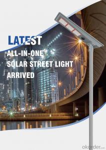
- Q:Can solar silicon wafers be used in solar-powered street lighting?
- Yes, solar silicon wafers can be used in solar-powered street lighting. These wafers are commonly used in the production of solar cells, which convert sunlight into electricity. Solar-powered street lighting systems utilize solar panels made with silicon wafers to generate electricity from the sun and power the street lights.
- Q:How much energy is needed to produce a solar silicon wafer?
- The amount of energy required to produce a solar silicon wafer can vary depending on several factors such as the manufacturing process, technology used, and efficiency of the production facility. However, on average, it is estimated that around 250-350 kilowatt-hours (kWh) of energy are needed to manufacture one square meter of a standard silicon wafer for solar panels.
- Q:In the silicon surface cleaning, there is a final step, the silicon chip into the 4% concentration of HF solution soak for five minutes, to hydrogen passivation treatment, and then rinse with deionized water after nitrogen drying,What is the role and mechanism of this hydrogen passivation?
- 0.5 ~ 1min in order to achieve the effect of removing the damage layer, at this timeCorrosion rate can reach 6 to 10um/min.In the polishing process to remove the damage layer on the basis to try to reduce, to prevent corrosion of the wafer was too thin.
1. Manufacturer Overview |
|
|---|---|
| Location | |
| Year Established | |
| Annual Output Value | |
| Main Markets | |
| Company Certifications | |
2. Manufacturer Certificates |
|
|---|---|
| a) Certification Name | |
| Range | |
| Reference | |
| Validity Period | |
3. Manufacturer Capability |
|
|---|---|
| a)Trade Capacity | |
| Nearest Port | |
| Export Percentage | |
| No.of Employees in Trade Department | |
| Language Spoken: | |
| b)Factory Information | |
| Factory Size: | |
| No. of Production Lines | |
| Contract Manufacturing | |
| Product Price Range | |
Send your message to us
Solar Cell High Quality A Grade Cell Polyrystalline 5v 16.0%
- Ref Price:
-
- Loading Port:
- Shanghai
- Payment Terms:
- TT OR LC
- Min Order Qty:
- 1000 pc
- Supply Capability:
- 100000 pc/month
OKorder Service Pledge
OKorder Financial Service
Similar products


New products
Hot products


Hot Searches
Related keywords