Specifications
1. Free technical support
2.Turnkey service
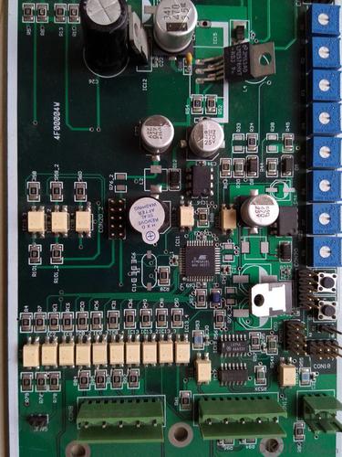
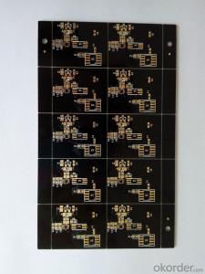
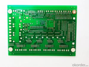
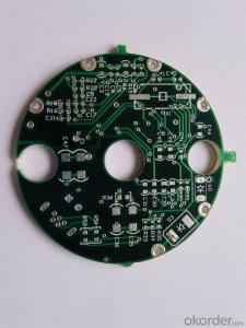
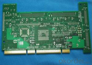
multi-layer pcb design and custom pcba
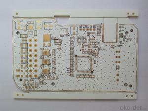
♥PCB Manufacture
Material: FR4, High TG FR4, Halogen Free material, Rogers HF material, etc.
Layer counts: 2-28 layers
Finished Copper Thickness: 0.5-5 OZ
Finished Board Thickness: 0.2-6.0mm
Min. Line/Track Width: 4mil
Min. Line/Track Space: 4mil
Min. Contour Tolerance: +/-0.1mm
Min. Finished Diameter of PTH Hole: 0.2mm
Max. Board Thickness/Hole Ratio: 12:1
Min. Solder Mask Bridge: 4mil (Min. SMT Pad Space 8mil)
Min. Legend (Silk screen) Track Width: 5mil
Min. Legend (Silk screen) Height: 30mil
Min. drilling slot size: 0.6mm
Solder mask color: green, black, blue, white, yellow, purple, and matt, etc.
Solder mask hardness: 6H
Legend/Silk screen Color: white, yellow, black, etc.
Surface Treatment: HAL, Lead Free HAL, Immersion gold, OSP, Immersion tin, Immersion silver, etc.
Other Technology: Gold finger, peelable mask, Non-across blind/buried vias, characteristic impedance control, Rigid-flex board etc.
Reliability Test: flying probe test/fixture test, impedance test, solderability test, thermal shock test, hole resistance test, and micro metallographic section analysis, etc.
Wrap and twist: ≤0
Flammability: 94V-0
4. Professional engineering staff to provide technical support.
5.OEM and ODM service are welcome.
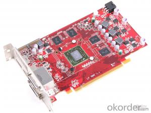
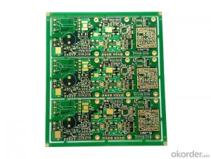
♥PCB Assembly
Military standard assembly
Minimum lead time for assembly is only 3 days
Turnkey service(PCB manufacture, components procurement and assembly)
Prototype building, No Minimum quantity Required
Reliable Parts
Surface mount, through hole, BGA, QFP, QFN …
ROHS compliant and lead-free process
OurPCB Profile:
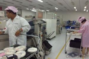
♣ OurPCB Tech Limited was found in 2005, it provides professional PCB&PCBA service for over than 1500 customers around the world. In order to satisfy more and more customers requirement about lead time and price, OurPCB built its own assembly factory in April 2011
♣ OurPCB's Assembly factory is equiped many advanced machines, e.g. Siemens HS50 placer, Siemens F5 Placer, Heller 1809 Reflow,Speedline MPM printer,OK intelligent solder iron,Otek Automatic Optical Inspection... we can assemble BGA,LGA,QFN,QFP,DIP,SIP...., The smallest package form we can mount is 0201. Our factory also can provide programming,wiring, screwing, injecting and conformal coating service. It have ISO9001 Certification
♣ For bare PCB manufacture, OurPCB is an important partner of Shenzhen Uniwell Circuits Co., Ltd www.uniwellcircuits.com, which have two PCB manufacture factories now, Uniwell have ISO9001, ISO14001,TS16949,UL certifications
♣ OurPCB Vision: Be the most reliable PCB and PCBA service supplier.
♣ OurPCB Mission:
Dedicate to satisfy customers' needs.
Provide high quality products
Provide most professional services.
Deliver products on time.
Keep all costs to minimum and maximize our customers' benefits.
Certifications:
♣ UL,16949, RoHS, ISO9001
♣ High layers PCB manufacturing, up to 32 layers
♣ Low costs, Minimum cost for 3 prototype boards is only $84!!!
♣ Fast service, Minimum lead time for bare PCB is only 2 days
♣ Promptly reply, quotation will be provided in 8 working hours!