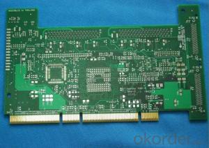


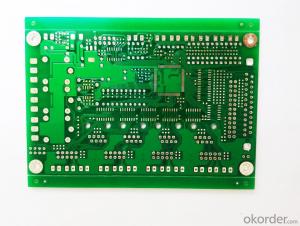
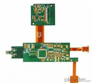
High quality 8 layer gold finger pcb, made in china
- Ref Price:
-

- Loading Port:
- Shanghai
- Payment Terms:
- TT OR LC
- Min Order Qty:
- 1 pc
- Supply Capability:
- 10000 pc/month
OKorder Service Pledge
OKorder Financial Service
You Might Also Like
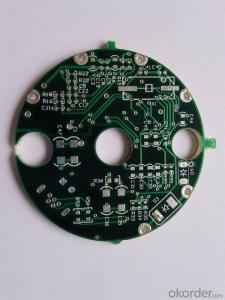
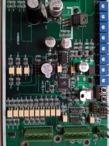
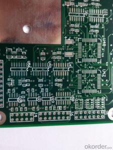
Specification

Product Description
1. UL,ISO9001,ISO14001, TS16949 certificate
2. Short lead time.
3. PCB ROHS compliant.
4. Turkey service
Free Technology Support
PCB Assembly
Turnkey service(PCB manufacture, components procurement and assembly)
Minimum lead time for assembly is only 5 days
Prototype building, No Minimum quantity Required
Reliable Parts
Surface mount, through hole, BGA, QFP, QFN …
ROHS compliant and lead-free process
PCB Capability
Material: FR4, CEM-3, Halogen Free, Rogers, High TG etc.
Layer counts: 1-18 layers
Finished Copper Thickness: 0.5-4 OZ
Finished Board Thickness: 0.2-5.0mm
Min. Line/Track Width: 4mil
Min. Line/Track Space: 4mil
Min. Contour Tolerance: +/-0.1mm
Min. Finished Diameter of PTH Hole: 0.2mm
Max. Board Thickness/Hole Ratio: 12:1
Min. Solder Mask Bridge: 4mil (Min. SMT Pad Space 8mil)
Min. Legend (Silk screen) Track Width: 5mil
Min. Legend (Silk screen) Height: 30mil
Min. drilling slot size: 0.6mm
Solder mask color: green, black, blue, white, yellow, purple, and matt, etc.
Legend/Silk screen Color: white, yellow, black, etc.
Surface Treatment: HAL, Lead Free HAL, Immersion gold, OSP, Immersion tin, Immersion silver, etc.
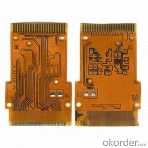
Other Technology: Gold finger, peelable mask, Non-across blind/buried vias, characteristic impedance control, Rigid-flex board etc.
Reliability Test: flying probe test/fixture test, impedance test, solderability test, thermal shock test, hole resistance test, and micro metallographic section analysis, etc.
Bow and twist: ≤1%
Flammability: 94V-0
4. Professional engineering staff to provide technical support.
5.OEM and ODM service are welcome.
Packaging Detail: Vacuum packaging
Delivery Time: 10-15 days
- Q: Circuit board display device which
- Through Hole: There are metal vias and non-metallic vias, where metal vias are used to connect the components between the layers of the pins.
- Q: Protel pcb how to rotate the board?
- It includes circuit schematic drawing, analog circuit and digital circuit mixed signal simulation, multi-layer printed circuit board design, programmable logic device design, chart generation,
- Q: Who can tell me printed circuit board in the multi-layer and double-sided panels and the difference between the single-layer, multi-layer between the layers is how the distribution?
- One side of the circuit, multilayer circuit board is between the board through the small hole connecting circuit `you carefully look at the multi-layer board` there are a lot of small holes above those holes in fact there are wires `is connected to a few boards
- Q: PCB printed circuit board, the "printed" is not referring to thermal transfer? Mass production PCB is also produced by thermal transfer method?
- Not the heat transfer, where the printing is an image of the argument, because the PCB line looks like the same as printed on the substrate.
- Q: Which boards are difficult boards?
- Printed circuit boards and semi-flexible printed circuit boards. Which HDI, rigid-flex relatively difficult. Because of its complex process, the process, equipment requirements are high.
- Q: How to eliminate the protection of IC on the circuit board paint
- his paint is treated at high temperature and is treated with solder resist. General chemical solvents can not be dissolved. Scratch or wipe off. With fine sandpaper.
- Q: Protel how to lock all components
- In the electronics industry CAD software, it deservedly ranked in front of many EDA software, is the preferred software for electronic designers, it began to use in the country earlier, the highest penetration rate in the country, and some colleges and universities of electronic professional also Special courses to learn it, almost all of the electronics companies have to use it, many large companies in the recruitment of electronic design talent in their conditions on the bar often asked to use PROTEL. Early PROTEL mainly used as a printed circuit board automatic routing tools,
- Q: There are several main circuit board process
- Material production - open material --- inner line - press - mechanical drilling - plating - outer line - anti-welding - text --- surface treatment - molding --- test - Appearance inspection --- packaging shipping
- Q: PCB circuit board? What is it?
- As electronic devices become more complex, more and more parts are needed, and the lines and parts on the PCB are becoming more and more dense. Bare boards (no parts on top) are also often referred to as "Printed Wiring Board (PWB)". The board itself is made of insulated and non-bendable material. On the surface you can see the small line material is copper foil,
- Q: Multilayer circuit boards, is not all power must be placed on the inner layer
- In addition, the surface of course can also put the ground, power, just because the device occupied the area of ??the reasons, not a complete layer. So many devices may not be able to take electricity.
Send your message to us
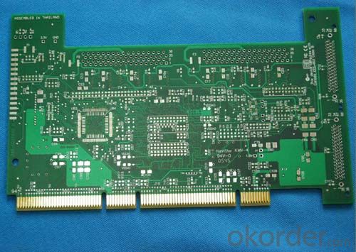
High quality 8 layer gold finger pcb, made in china
- Ref Price:
-
- Loading Port:
- Shanghai
- Payment Terms:
- TT OR LC
- Min Order Qty:
- 1 pc
- Supply Capability:
- 10000 pc/month
OKorder Service Pledge
OKorder Financial Service
Similar products
Hot Searches
Related keywords

