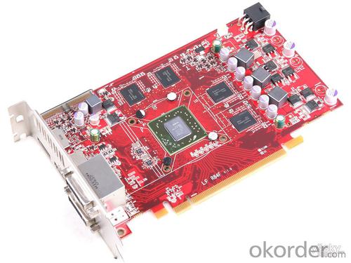
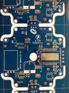
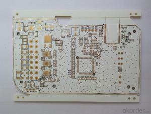
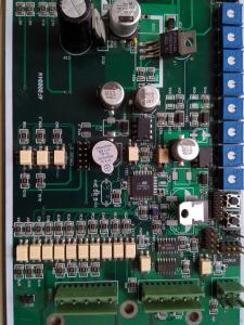
• multilayer PCB fabrication/design/assembly System 1
  • multilayer PCB fabrication/design/assembly System 2
  • multilayer PCB fabrication/design/assembly System 3
multilayer PCB fabrication/design/assembly

multilayer PCB fabrication/design/assembly

Ref Price:
get latest price
Loading Port:
Shanghai
Payment Terms:
TT OR LC
Min Order Qty:
1 pc
Supply Capability:
10000 pc/month

Add to My Favorites

Follow us:


OKorder Service Pledge

Quality Product, Order Online Tracking, Timely Delivery

OKorder Financial Service

Credit Rating, Credit Services, Credit Purchasing

Specification

Base material:
FR4 TG170
Board thickness:
1.6mm±10%
Copper thickness:
1oz
IPC Class:
Class 2
Min trace/gap:
4mil/4mil
Min hole:
0.2mm
Surface finish:
ENIG(2u'')

Product Description:


Quick Details

  • Place of Origin: Shanghai, China (Mainland)

  • Brand Name: OEM

  • Model Number: Customized

  • Base Material: FR4

  • Copper Thickness: 1oz

  • Board Thickness: 1.6mm±10%

  • Min. Hole Size: 0.2mm

  • Min. Line Width: 4mil

  • Min. Line Spacing: 4mil

  • Surface Finishing: HAL,Lead Free HAL,ENIG(2u''),OSP,Immersion tin,Immersion silver

  • solder mask color: green, red, blue, black

  • Certificate: ISO9001, ISO14001,TS16949, UL certifications

Packaging & Delivery

Packaging Details:vacuum packing, anti-static package or in your requirement
Delivery Detail:10-15days after payment by DHL/FedEx/EMS or you need

Specifications

PCBA 
1.Low cost, Minimum cost for 3 prototypes PCB is $80 only. 
2.Short lead time. 
3.PCB ROHS compliant. 
4.Turkey service 

Free Technology Support
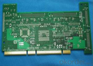

PCB Assembly

             Military standard assembly

             Minimum lead time for assembly is only 3 days

             Turnkey service(PCB manufacture, components procurement and assembly)

             Prototype building, No Minimum quantity Required

             Reliable Parts

             Surface mount, through hole, BGA, QFP, QFN …

             ROHS compliant and lead-free process
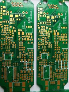
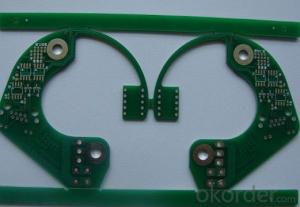
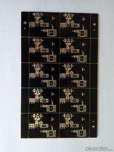
PCB Capability


Material: FR4, CEM-3, Aluminum base, Halogen Free material, Rogers, High TG etc.

Layer counts: 2-18 layers

Finished Copper Thickness: 0.5-4 OZ

Finished Board Thickness: 0.2-5.0mm

Min. Line/Track Width: 4mil

Min. Line/Track Space: 4mil

Min. Contour Tolerance: +/-0.1mm

Min. Finished Diameter of PTH Hole: 0.2mm

Max. Board Thickness/Hole Ratio: 12:1

Min. Solder Mask Bridge: 4mil (Min. SMT Pad Space 8mil)

Min. Legend (Silk screen) Track Width: 5mil

Min. Legend (Silk screen) Height: 30mil

Min. drilling slot size: 0.6mm

Solder mask color: green, black, blue, white, yellow, purple, and matt, etc.

Solder mask hardness: 6H

Legend/Silk screen Color: white, yellow, black, etc.

Surface Treatment: HAL, Lead Free HAL, Immersion gold, OSP, Immersion tin, Immersion silver, etc.

Other Technology: Gold finger, peelable mask, Non-across blind/buried vias, characteristic impedance control, Rigid-flex board etc.

Reliability Test: flying probe test/fixture test, impedance test, solderability test, thermal shock test, hole resistance test, and micro metallographic section analysis, etc.

Wrap and twist: ≤0

Flammability: 94V-0

4. Professional engineering staff to provide technical support.

5.OEM and ODM service are welcome.

Q: What is the light blue oil component used for brush circuit boards
Printed circuit board manufacturing process is developing rapidly, and different types of PCBs require different technologies, but the basic method is the same.
Q: PCB (double-sided multi-layer printed circuit board) about the production principle of what?
(Cut through the production unit) -> drilling (drilling through hole) -> copper (copper on the hole, the principle is the palladium ion) -> plate power (thickening table / hole copper thick) ->
Q: What does the printed motherboard mean?
As the printed circuit board is not a general terminal product, so the name of the definition of a little confusion, such as: personal computer motherboard, called the motherboard, and can not be directly called the circuit board, although the motherboard board there is a circuit board, but
Q: Circuit board how to see the line
For example, you say the TV part of its circuit is divided into: power part / high-frequency head part / IF frequency amplification / video detection part / part of the partial / line scan / high voltage part / audio circuit / color decoding circuit.
Q: Pcb board on the big black dot chip package called what?
Its development has been 100 years of history; its design is mainly layout design; the main advantage of using the circuit board is to greatly reduce the wiring and assembly errors, improve the level of automation and production labor rate.
Q: What are the materials used for the Merrillas on PCB circuit boards?
Its development has been 100 years of history; its design is mainly layout design; the main advantage of using the circuit board is to greatly reduce the wiring and assembly errors, improve the level of automation and production labor rate. According to the number of circuit board can be divided into single-sided, double-sided, four-tier, six-board and other multi-layer circuit boards.
Q: PCB board can be stored for how long
For example: because there are integrated circuit parts loaded on the circuit board, so the news media called him IC board, but in essence he is not the same as the printed circuit board. We usually say that the printed circuit board refers to the bare board - that is, no components on the circuit board.
Q: What is the working principle of the circuit board?
the circuit board to make the circuit mini, visualization, for the fixed circuit production and optimization of electrical appliances play an important role in the layout. The circuit board can be called printed circuit board or printed circuit board, the English name is (Printed Circuit Board) PCB.
Q: Just start learning computer hardware maintenance technology, only know the melting point of tin is 230 degrees Celsius, if the PCB board unloading capacitor resistors and other components, then the hot air gun should be transferred to a few degrees Celsius will not damage the PCB board?
As the printed circuit board is not a general terminal product, so the name of the definition of a little confusion, such as: personal computer motherboard, called the motherboard, and can not be directly called the circuit board, although the motherboard board there is a circuit board, but Is not the same, so the assessment of the industry when the two can not say the same. For example: because there are integrated circuit parts loaded on the circuit board, so the news media called him IC board, but in essence he is not the same as the printed circuit board. Generally speaking, the printed circuit board refers to the bare board - that is, no upper components of the circuit board.
Q: Multilayer circuit boards, is not all power must be placed on the inner layer
Multi-layer circuit board, not all power must be placed on the inner layer, the internal layer can also be traced.

Send your message to us

This is not what you are looking for? Post Buying Request

Similar products

Hot products


Hot Searches

Related keywords