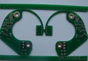
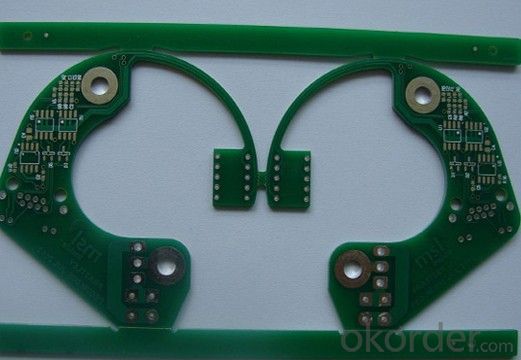
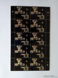
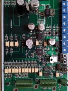
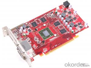
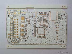
• PCB fab 2-20 layers System 1
  • PCB fab 2-20 layers System 2
  • PCB fab 2-20 layers System 3
PCB fab 2-20 layers

PCB fab 2-20 layers

Ref Price:
get latest price
Loading Port:
Qingdao
Payment Terms:
TT OR LC
Min Order Qty:
-
Supply Capability:
-

Add to My Favorites

Follow us:


OKorder Service Pledge

Quality Product, Order Online Tracking, Timely Delivery

OKorder Financial Service

Credit Rating, Credit Services, Credit Purchasing

Quick Details

  • Place of Origin: Hebei, China (Mainland)

  • Brand Name: OEM

  • Model Number: customized

  • Number of Layers: 1-32

  • Base Material: FR4 CEM-9 Rogers HF

  • Copper Thickness: 0.5-5 OZ

  • Board Thickness: 0.2-6.0mm

  • Min. Hole Size: 0.2mm

  • Min. Line Width: 4mil

  • Min. Line Spacing: 4mil

  • Surface Finishing: hal immersion gold immersion silver OSP

  • color: red ,green ,yellow, black, white

Packaging & Delivery

Packaging Details:vaccum / anti-static in carton or as your requirement
Delivery Detail:within 20 days after getting your payment

Specifications

electronic test PCB
a. PCB OEM&ODM
b. PCB Clone/Copy,Design
d. Turnkey service
e. UL,SGS,RoSH,TS certificate
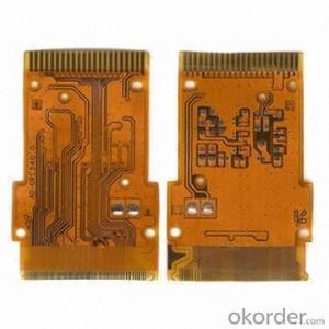
 PCB Manufacturer

OurPCB Technical capabilities

NO

ITEM

Technical capabilities

1

Layers

2-20 layers

2

Max. Board size

2000×610mm

3

Min. board Thickness

2-layer  0.15mm

4-layer  0.38mm

6-layer  0.55mm

8-layer  0.80mm

10-layer  1.0mm

4

Min. line Width/Space

0.075mm(3mil)

5

Max. Copper thickness

6OZ

6

Min. S/M Pitch

0.075mm(3mil)

7

Min. hole size

0.1mm(4mil)

8

Hole dia. Tolerance (PTH)

±0.05mm(2mil)

9

Hole dia. Tolerance (NPTH)

+0/-0.05mm(2mil)

10

Hole position deviation

±0.05mm(2mil)

11

Outline tolerance

±0.10mm(4mil)

12

Twist & Bent

0.75%

13

Insulation Resistance

>1012 Ω Normal

14

Electric strength

>1.3kv/mm

15

S/M abrasion

>6H

16

Thermal stress

288°C 20Sec

17

Test Voltage

50-300V

18

Min. blind/buried via

0.15mm  (6mil)

19

Surface Finished

HAL, ENIG, ImAg, Imsn OSP, Plating AG, Plating gold

20

Materials

FR4,H-TG,Teflon,Rogers,Ceramics,Aluminium, Copper base


Q: What is the processing of waste printed circuit boards?
Hebei Cangzhou Lida circuit board factory mainly produces single-sided circuit boards, circuit boards, aluminum circuit board, PCB circuit board, circuit boards, LED circuit board and multi-layer circuit board, and is widely used in aerospace, defense, communications, home appliances, environmental protection, medical and industrial control field.
Q: What are the classifications of PCB?
The number of layers of the board does not mean that there are several layers of independent wiring layer, in particular, will be added to the empty layer to control the thickness of the plate, usually even number of layers, and contains the outermost two layers. Most of the motherboard is 4 to 8 layers of the structure, but the technical theory can do nearly 100 layers of PCB board. Most large supercomputers use very high levels of motherboards, but since such computers can already be replaced by clusters of many ordinary computers, the multi - layer board is gradually being used. Because the PCB in each layer are closely integrated, it is not easy to see the actual number, but if you look at the motherboard, you can see.
Q: What are the circuit board technology?
The circuit board can be called a printed circuit board or printed circuit board, English name (Printed Circuit Board), PCB (Flexible Printed Circuit board [1] (FPC) FPC circuit board circuit board and flexible circuit board flexible circuit board is made of polyimide or polyester film as a base material with high reliability, excellent can flexible printed circuit board. It has the characteristics of high density, light weight, thin thickness and good flexibility And soft and hard board (reechas, Soft hard combination plate) -FPC and the birth and development of PCB, gave birth to the hard and soft combination board this new product. Therefore, the combination of soft and hard board, that is, flexible circuit board and rigid circuit board, after pressing the process, according to the relevant requirements of the process together to form a circuit board with FPC characteristics and PCB characteristics.
Q: What are the classification of circuit boards?
According to the characteristics of the circuit board if divide into soft board (FPC), and (PCB), flex board (FPCB).
Q: Printed circuit board, double-sided printing or single-sided printing? What is the difference?
Because the wire is only one side of it, we call this PCB a single circuit board. Because there are a lot of strict restrictions on the design of the circuit board (because there is only one side, the wiring can not be * * * * * * and must be around the path alone.
Q: Why PCB circuit board components should be placed on one side
Because the discrete components of the welding foot to wave soldering, that is to say: the other side of the PCB plate from the tin bath,
Q: What are the abnormal quality of circuit board development?
The first is a single panel, in the most basic PCB, the parts are concentrated in one side, the conductor is concentrated on the other side. Because the wire only appears on one side, it is called the PCB. Single panel is usually simple, low cost, but the drawback is that it can not be applied to complex products.
Q: What circuit board belongs to difficulty board? Why?
If the circuit board according to the product classification, a single-sided printed circuit board, double-sided printed circuit boards, multilayer printed circuit board, HDI high density PCB, flexible printed circuit board, flex type printed circuit board and semi flexible printed circuit board etc..
Q: Circuit board production process is what?
After the completion of the inner circuit board must be glass fiber resin film and the outer circuit copper foil adhesive. Before pressing, the inner plate needs to be treated by black (oxygen), so as to increase the insulation of the copper surface, and to make the inner surface of the copper wire rough so as to produce good adhesion with the film. The inner superposed circuit board six layer lines, containing more than was paired with rivet riveting machine. And then put it on the plate, and put it in the mirror steel plate, into the vacuum press in the appropriate temperature and pressure to harden the film adhesive. After the pressure circuit board with X light automatic positioning drill drill hole hole as the reference target drone for outer line alignment. And the edge of the plate to do the appropriate cutting, in order to facilitate subsequent processing.
Q: PCB board single-sided electronic parts and double-sided electronic parts price difference
However, the general manufacturers have a charging standard, manufacturers are different, the charges are different, or to ask manufacturers more reliable.

Send your message to us

This is not what you are looking for? Post Buying Request

Similar products

Hot products


Hot Searches