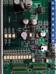
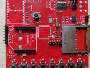
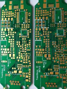
• pcb antenna customize pcba single sided pcb design System 1
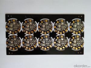
  • pcb antenna customize pcba single sided pcb design System 2
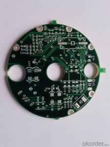
  • pcb antenna customize pcba single sided pcb design System 3
  • pcb antenna customize pcba single sided pcb design System 4
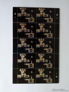
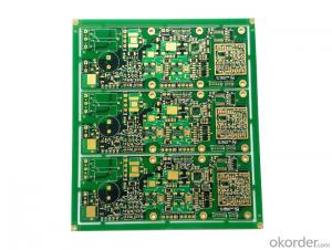
pcb antenna customize pcba single sided pcb design

pcb antenna customize pcba single sided pcb design

Ref Price:
get latest price
Loading Port:
China Main Port
Payment Terms:
TT OR LC
Min Order Qty:
-
Supply Capability:
-

Add to My Favorites

Follow us:


OKorder Service Pledge

Quality Product, Order Online Tracking, Timely Delivery

OKorder Financial Service

Credit Rating, Credit Services, Credit Purchasing

Quick Details

  • solder mask color: green

  • certificate: ISO9001, ISO14001,TS16949, UL certifications

  • Packaging: vacuum packing, anti-static package

  • Delivery: 10-15 days after your payment

  • MOQ: 1 Piece

  • Payment: T/T,Western Union,Paypal

  • shipping term: by FEDEX/DHL/EMS/TNT/UPS

Packaging & Delivery

Packaging Details:anti-static packing, vacuum packing, carton packing
Delivery Detail:10-15days after payment by DHL/FedEx/EMS or you need

Specifications

1. Free technical support
2.Turnkey service

pcb antenna  customize pcba single sided pcb design  

♥PCB Manufacture

Material: FR4, High TG FR4, Halogen Free material, Rogers HF material, etc.

Layer counts: 2-28 layers

Finished Copper Thickness: 0.5-5 OZ

Finished Board Thickness: 0.2-6.0mm

Min. Line/Track Width: 4mil

Min. Line/Track Space: 4mil

Min. Contour Tolerance: +/-0.1mm

Min. Finished Diameter of PTH Hole: 0.2mm

Max. Board Thickness/Hole Ratio: 12:1

Min. Solder Mask Bridge: 4mil (Min. SMT Pad Space 8mil)

Min. Legend (Silk screen) Track Width: 5mil

Min. Legend (Silk screen) Height: 30mil

Min. drilling slot size: 0.6mm

Solder mask color: green, black, blue, white, yellow, purple, and matt, etc.

Solder mask hardness: 6H

Legend/Silk screen Color: white, yellow, black, etc.

Surface Treatment: HAL, Lead Free HAL, Immersion gold, OSP, Immersion tin, Immersion silver, etc.

Other Technology: Gold finger, peelable mask, Non-across blind/buried vias, characteristic impedance control, Rigid-flex board etc.

Reliability Test: flying probe test/fixture test, impedance test, solderability test, thermal shock test, hole resistance test, and micro metallographic section analysis, etc.

Wrap and twist: ≤0

Flammability: 94V-0

4. Professional engineering staff to provide technical support.

5.OEM and ODM service are welcome.


♥PCB Assembly

             Military standard assembly


             Minimum lead time for assembly is only 3 days


             Turnkey service(PCB manufacture, components procurement and assembly)


             Prototype building, No Minimum quantity Required


             Reliable Parts


             Surface mount, through hole, BGA, QFP, QFN


             ROHS compliant and lead-free process


OurPCB Profile:

♣    OurPCB Tech Limited was found in 2005, it provides professional PCB&PCBA service for over than 1500 customers around the world. In order to satisfy more and more customers requirement about lead time and price, OurPCB built its own assembly factory in April 2011


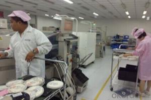
♣    OurPCB's Assembly factory is equiped many advanced machines, e.g. Siemens HS50 placer, Siemens F5 Placer, Heller 1809 Reflow,Speedline MPM printer,OK intelligent solder iron,Otek Automatic Optical Inspection... we can assemble BGA,LGA,QFN,QFP,DIP,SIP...., The smallest package form we can mount is 0201. Our factory also can provide programming,wiring, screwing, injecting and conformal coating service. It have ISO9001 Certification


♣    For bare PCB manufacture, OurPCB is an important partner of Shenzhen Uniwell Circuits Co., Ltd www.uniwellcircuits.com, which have two PCB manufacture factories now, Uniwell have ISO9001, ISO14001,TS16949,UL certifications


♣    OurPCB Vision: Be the most reliable PCB and PCBA service supplier.

♣    OurPCB Mission:

  • Dedicate to satisfy customers' needs.

  • Provide high quality products

  • Provide most professional services.

  • Deliver products on time.

  • Keep all costs to minimum and maximize our customers' benefits.

Certifications:

♣  UL,16949, RoHS, ISO9001


♣  High layers PCB manufacturing, up to 32 layers


♣  Low costs, Minimum cost for 3 prototype boards is only $84!!!


♣  Fast service, Minimum lead time for bare PCB is only 2 days


♣  Promptly reply, quotation will be provided in 8 working hours!

Q: What are the classifications of PCB?
With a double and two single block as inner layer as the outer layer or two double-sided printed circuit board for the outer layer of the inner layer, two single block, through the positioning system and an insulating adhesive material alternately printed circuit board according to the design requirements for interconnection together and the conductive pattern becomes the four layer, six layer printed circuit board, also known as for multilayer printed circuit board.
Q: What are the circuit board technology?
The circuit board can be called a printed circuit board or printed circuit board, English name (Printed Circuit Board), PCB (Flexible Printed Circuit board [1] (FPC) FPC circuit board circuit board and flexible circuit board flexible circuit board is made of polyimide or polyester film as a base material with high reliability, excellent can flexible printed circuit board. It has the characteristics of high density, light weight, thin thickness and good flexibility And soft and hard board (reechas, Soft hard combination plate) -FPC and the birth and development of PCB, gave birth to the hard and soft combination board this new product. Therefore, the combination of soft and hard board, that is, flexible circuit board and rigid circuit board, after pressing the process, according to the relevant requirements of the process together to form a circuit board with FPC characteristics and PCB characteristics.
Q: What is the difference between single and double side of cement pressure plate?
Cement board is ordinary cement pouring pressure, pressure resistance is not high
Q: How to make a complete circuit version?
The stencil tile in the steel plate, the plate will pen drawing according to the ratio of 1:1 in a stencil, stencil plate diagram according to the size of the circuit board cut, and the flat on the copper clad plate. With a small amount of paint and talcum powder into thin thick suitable materials, with a brush dipped in India mixed materials, evenly coated with wax paper, repeated several times, can be printed on the printed circuit board (laminate).
Q: What is the use of circuit boards?
The circuit board makes the circuit miniaturization and intuitive, and plays an important role in the mass production and optimization of the electrical layout of the fixed circuit.
Q: What does PCB mean?
Because it is made of electronic printing, it is called "printed" circuit board.
Q: How to distinguish the circuit board is a single-sided or double-sided or multilayer board?
The multilayer board refers to a circuit board which is provided with 3 layers or more than 3 layers to be pressed together, and the double panel is that one side of a plate is provided with a circuit. Carefully observe the multilayer board, there are a lot of small holes, which are actually inside the wire is connected to a few boards on both sides of the board but also less.
Q: PCB what material?
Copper clad phenolic glass cloth laminate is non alkali glass cloth laminate impregnated with epoxy phenolic resin formed by hot pressing, one or both sides coated with copper foil, has the advantages of light weight, good electrical and mechanical properties, easy processing etc.. The surface of the plate is light yellow, and if the three cyanogen amine is used as a curing agent, the surface of the plate is light green and has good transparency. Printed circuit boards are mainly used in radio equipment with high operating temperature and operating frequency.
Q: What is a single-sided circuit board?
Single sided circuit board refers to the most basic PCB, the parts are concentrated in one side, the conductor is concentrated on the other side, the wire only in one side of the meaning.
Q: What is the best PCB circuit board
The "bridge" between such circuits is called a guide hole (via). A guide hole is a small hole filled or coated with metal on PCB, which can be connected to a wire on both sides. Because the double sided area than a single panel doubled, double panel solves the single panel because of difficult wiring staggered (through hole conduction to the other side), it is more suitable for use in circuit is more complex than a single panel.

Send your message to us

This is not what you are looking for? Post Buying Request

Similar products

Hot products


Hot Searches