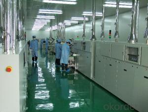


Solar Cell High Quality A Grade Cell Polyrystalline 5v 15.6%
- Ref Price:
-

- Loading Port:
- Shanghai
- Payment Terms:
- TT OR LC
- Min Order Qty:
- 1000 pc
- Supply Capability:
- 100000 pc/month
OKorder Service Pledge
OKorder Financial Service
You Might Also Like


Specifications
hot sale solar cell
1.16.8%~18.25% high efficiency
2.100% checked quality
3.ISO9001/ISO14001/TUV/CE/UL
4.stable performance
We can offer you the best quality products and services, don't miss !
POLY6'(156*156)
Polycrystalline Silicon Solar cell
Physical Characteristics
Dimension: 156mm×156mm±0.5mm
Diagonal: 220mm±0.5mm
Thickness(Si): 200±20 μm
Front(-) Back(+)
Blue anti-reflecting coating (silicon nitride); Aluminum back surface field;
1.5mm wide bus bars; 2.0mm wide soldering pads;
Distance between bus bars: 51mm . Distance between bus bars :51mm .
Electrical Characteristics
Efficiency(%) | 18.00 | 17.80 | 17.60 | 17.40 | 17.20 | 16.80 | 16.60 | 16.40 | 16.20 | 16.00 | 15.80 | 15.60 |
Pmpp(W) | 4.33 | 4.29 | 4.24 | 4.19 | 4.14 | 4.09 | 4.04 | 3.99 | 3.94 | 3.90 | 3.86 | 3.82 |
Umpp(V) | 0.530 | 0.527 | 0.524 | 0.521 | 0.518 | 0.516 | 0.514 | 0.511 | 0.509 | 0.506 | 0.503 | 0.501 |
Impp(A) | 8.159 | 8.126 | 8.081 | 8.035 | 7.990 | 7.938 | 7.876 | 7.813 | 7.754 | 7.698 | 7.642 | 7.586 |
Uoc(V) | 0.633 | 0.631 | 0.628 | 0.625 | 0.623 | 0.620 | 0.618 | 0.617 | 0.615 | 0.613 | 0.611 | 0.609 |
Isc(A) | 8.709 | 8.677 | 8.629 | 8.578 | 8.531 | 8.478 | 8.419 | 8.356 | 8.289 | 8.220 | 8.151 | 8.083 |

MONO5'(125*125mm)165
Monocrystalline silicon solar cell
Physical Characteristics
Dimension: 125mm×125mm±0.5mm
Diagonal: 165mm±0.5mm
Thickness(Si): 200±20 μm
Front(-) Back(+)
Blue anti-reflecting coating(silicon nitride); Aluminum back surface field;
1.6mmwide bus bars; 2.5mm wide soldering pads;
Distance between bus bars: 61mm . Distance between bus bars :61mm .
Electrical Characteristics
Efficiency(%) | 19.40 | 19.20 | 19.00 | 18.80 | 18.60 | 18.40 | 18.20 | 18.00 | 17.80 | 17.60 | 17.40 | 17.20 |
Pmpp(W) | 2.97 | 2.94 | 2.91 | 2.88 | 2.85 | 2.82 | 2.79 | 2.76 | 2.73 | 2.70 | 2.67 | 2.62 |
Umpp(V) | 0.537 | 0.535 | 0.533 | 0.531 | 0.527 | 0.524 | 0.521 | 0.518 | 0.516 | 0.515 | 0.513 | 0.509 |
Impp(A) | 5.531 | 5.495 | 5.460 | 5.424 | 5.408 | 5.382 | 5.355 | 5.328 | 5.291 | 5.243 | 5.195 | 4.147 |
Uoc(V) | 0.637 | 0.637 | 0.636 | 0.635 | 0.633 | 0.630 | 0.629 | 0.629 | 0.628 | 0.626 | 0.626 | 0.625 |
Isc(A) | 5.888 | 5.876 | 5.862 | 5.848 | 5.839 | 5.826 | 5.809 | 5.791 | 5.779 | 5.756 | 5.293 | 5.144 |

FAQ:
Q:How can i get some sample?
A:Yes , if you want order ,sample is not a problem.
Q:How about your solar panel efficency?
A: Our product efficency around 17.25%~18.25%.
Q:What’s the certificate you have got?
A: we have overall product certificate of ISO9001/ISO14001/CE/TUV/UL
- Q:Can solar silicon wafers be repaired?
- Yes, solar silicon wafers can be repaired to some extent. Minor damages like scratches and cracks can be repaired using various techniques such as polishing or filling with epoxy. However, significant damages or functional defects may require the replacement of the entire wafer. It is important to note that the repair process should be conducted by professionals to ensure the optimal performance and safety of the solar panel.
- Q:Can solar silicon wafers be used in underwater solar energy systems?
- Yes, solar silicon wafers can be used in underwater solar energy systems. However, special precautions need to be taken to ensure the wafers are properly sealed to prevent water damage and corrosion. Additionally, the design of the system should consider factors such as buoyancy, water pressure, and maintenance requirements in underwater environments.
- Q:Can solar silicon wafers be used in art installations?
- Yes, solar silicon wafers can be used in art installations. These wafers can be creatively incorporated into various artistic designs to add a unique and sustainable element to the installation.
- Q:Can solar silicon wafers be used in building-integrated photovoltaics?
- Yes, solar silicon wafers can be used in building-integrated photovoltaics (BIPV). BIPV systems are designed to seamlessly integrate solar panels into the building's structure, such as windows, walls, or roofs. Solar silicon wafers, which are the key component of traditional solar panels, can be specially designed and adapted to fit into BIPV applications, allowing for the generation of electricity while also serving as a functional building material.
- Q:How are solar silicon wafers protected from scratches during handling?
- Solar silicon wafers are typically protected from scratches during handling by using various methods such as applying a protective coating or using specially designed handling equipment.
- Q:What is the thickness of the semiconductor wafer used today?I have consulted some for solar wafers, heard now that the wafer thickness in 200~400 micron, but we need the wafer thickness requirements for high now, that for semiconductor wafer thickness is slightly higher than the solar energy, but I do not know how much is there in about 1 mm
- We do DIP package, 4 inch wafer to be thin to 0.300mm; 6 inch wafer to be reduced to about 0.320mm, error 0.020mm.
- Q:Can solar silicon wafers be used in building-integrated photovoltaics (BIPV)?
- Yes, solar silicon wafers can be used in building-integrated photovoltaics (BIPV). BIPV refers to the integration of solar panels or cells into the building envelope, such as windows, roofs, or facades. Silicon wafers are commonly used in the production of solar cells, including those used in BIPV systems. These wafers are processed to create solar cells, which can then be integrated into various building materials, allowing for the generation of solar power while also serving as functional building elements.
- Q:How do solar silicon wafers perform in coastal areas?
- Solar silicon wafers generally perform well in coastal areas as long as they are properly protected against the corrosive effects of saltwater and strong winds.
- Q:Monocrystalline silicon processing technology
- Wafer thickness is also a factor in productivity, as it relates to the number of wafers produced by each silicon block. The ultrathin wafer presents additional challenges to the wire technology, because the production process is much more difficult to. In addition to the mechanical brittleness of silicon wafers, if the wire sawing process no precise control, slight crack and bending will have negative effects on product yield. The system must be of ultra-thin silicon wire technology, linear cutting line speed and pressure, and precise control of cutting coolant.Regardless of the thickness of the silicon wafer, crystal silicon solar cell manufacturers have made great demands on the quality of the silicon wafer. The wafer cannot have surface damage (minor cracks, wire mark), morphology defects (bending, convex, uneven thickness) to minimize additional back-end processing such as polishing and other requirements to a minimum. Current situationIn order to meet the market for lower cost and higher productivity, a new generation of wire must improve the cutting speed, the use of silicon longer so as to improve the cutting load. Thinner cutting lines and thinner silicon chips increase productivity, while advanced process control can manage cutting line tension to keep the cutting line firm.
- Q:What are the advantages of using a solar silicon wafer?
- One of the main advantages of using a solar silicon wafer is its high efficiency in converting sunlight into electricity. Silicon wafers have excellent electrical properties and can absorb a wide range of solar wavelengths, maximizing energy conversion. Additionally, silicon is abundant and readily available, making it a cost-effective option for solar panel manufacturing. Furthermore, silicon wafers are durable and have a long lifespan, ensuring reliable power generation for many years.
1. Manufacturer Overview |
|
|---|---|
| Location | |
| Year Established | |
| Annual Output Value | |
| Main Markets | |
| Company Certifications | |
2. Manufacturer Certificates |
|
|---|---|
| a) Certification Name | |
| Range | |
| Reference | |
| Validity Period | |
3. Manufacturer Capability |
|
|---|---|
| a)Trade Capacity | |
| Nearest Port | |
| Export Percentage | |
| No.of Employees in Trade Department | |
| Language Spoken: | |
| b)Factory Information | |
| Factory Size: | |
| No. of Production Lines | |
| Contract Manufacturing | |
| Product Price Range | |
Send your message to us
Solar Cell High Quality A Grade Cell Polyrystalline 5v 15.6%
- Ref Price:
-
- Loading Port:
- Shanghai
- Payment Terms:
- TT OR LC
- Min Order Qty:
- 1000 pc
- Supply Capability:
- 100000 pc/month
OKorder Service Pledge
OKorder Financial Service
Similar products


New products
Hot products


Related keywords