• specialized PCB and PCBA manufacturer System 1
  • specialized PCB and PCBA manufacturer System 2
  • specialized PCB and PCBA manufacturer System 3
specialized PCB and PCBA manufacturer

specialized PCB and PCBA manufacturer

Ref Price:
get latest price
Loading Port:
China Main Port
Payment Terms:
TT OR LC
Min Order Qty:
-
Supply Capability:
-

Add to My Favorites

Follow us:


OKorder Service Pledge

Quality Product, Order Online Tracking, Timely Delivery

OKorder Financial Service

Credit Rating, Credit Services, Credit Purchasing

Quick Details

  • Place of Origin: Hebei, China (Mainland)

  • Brand Name: OEM

  • Model Number: PCBA

  • Number of Layers: 2-28 layer

  • Base Material: FR-4

  • Copper Thickness: 1oz

  • Board Thickness: 1.6mm

  • Min. Hole Size: 0.1mm

  • Min. Line Width: 0.1mm

  • Min. Line Spacing: 0.075mm

  • Surface Finishing: HAL immersion gold immersion silver

  • color: green, blue, black, red

  • certificate: ISO9001, ISO14001,TS16949, UL certifications

Packaging & Delivery

Packaging Details:vacuum packing, anti-static package or in your requirement
Delivery Detail:10-15days after payment by DHL/FedEx/EMS or you need

Specifications

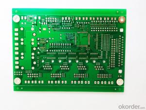
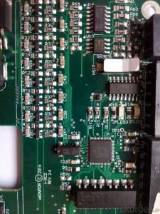
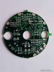
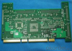
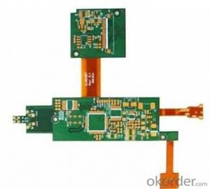
PCB layout ,PCB PCBA and Circuit assembly
1.Competitive price
2. On time delivery
3.NO MOQ
4. Turnkey service

Free Technology Support

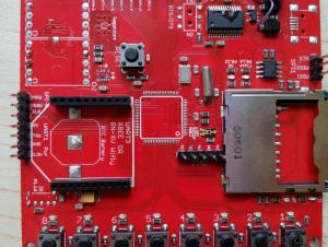
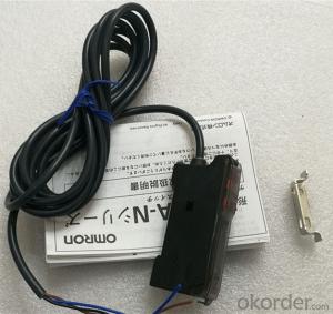
PCBA and PCBA Assembly, Suitable for Electronic Products

PCB service:

customized in controller with UL

1. OEM and ODM services are welcome

2. Approval: ISO9001:2008 UL, 16949, RoHS,

3. Quotation in 2 working days

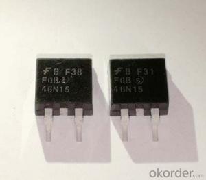
4. Complicated boards and components are also available

8. Adopted the advanced production equipments and testing instruments,

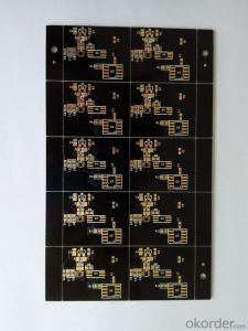
9.High layers PCB manufacturing, up to 36 layers.
10 Low costs, Minimum cost for 3 prototype boards is only $84!!!
11. Fast service, minimum lead time for bare PCB is only 2 days

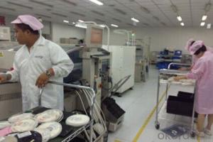
Leadsintec specializes in producing the various electronic products based on your customized designs and do pcba, pcb assembly for all kinds of small ,medium Volume electronic products


PCB Assembly

             Military standard assembly

             Minimum lead time for assembly is only 3 days

             Turnkey service(PCB manufacture, components procurement and assembly)

             Prototype building, No Minimum quantity Required

             Reliable Parts

             Surface mount, through hole, BGA, QFP, QFN …

             ROHS compliant and lead-free process

PCB Capability

Material: FR4, High TG FR4, Halogen Free material, Rogers HF material, etc.

Layer counts: 2-28 layers

Finished Copper Thickness: 0.5-5 OZ

Finished Board Thickness: 0.2-6.0mm

Min. Line/Track Width: 4mil

Min. Line/Track Space: 4mil

Min. Contour Tolerance: +/-0.1mm

Min. Finished Diameter of PTH Hole: 0.2mm

Max. Board Thickness/Hole Ratio: 12:1

Min. Solder Mask Bridge: 4mil (Min. SMT Pad Space 8mil)

Min. Legend (Silk screen) Track Width: 5mil

Min. Legend (Silk screen) Height: 30mil

Min. drilling slot size: 0.6mm

Solder mask color: green, black, blue, white, yellow, purple, and matt, etc.

Solder mask hardness: 6H

Legend/Silk screen Color: white, yellow, black, etc.

Surface Treatment: HAL, Lead Free HAL, Immersion gold, OSP, Immersion tin, Immersion silver, etc.

Other Technology: Gold finger, peelable mask, Non-across blind/buried vias, characteristic impedance control, Rigid-flex board etc.

Reliability Test: flying probe test/fixture test, impedance test, solderability test, thermal shock test, hole resistance test, and micro metallographic section analysis, etc.

Wrap and twist: ≤0

Flammability: 94V-0

4. Professional engineering staff to provide technical support.

5.OEM and ODM service are welcome.


Q:Protel do PCB circuit board, how to make the back of the double panel also has components
Double-sided are over reflow, the need for high and low temperature, high temperature surface to avoid electrolytic capacitors, smt high temperature surface solder paste, and then smt low temperature surface solder paste, low temperature surface can send those relatively heavy electrolytic capacitors and inductors such as the original Under the machine all the manual welding, processing costs are relatively high.
Q:On the PCB shop copper problem, if it is a double panel, is not also do not have to layout the ground, both sides of the shop copper, and finally casually playing some holes?
See you this "casually playing some of the hole", I think I have also thought that. Long time later to understand that those holes are pay attention to, but in the ordinary low frequency board is not so strict requirements only.
Q:What is the type of sheet material for double panels
According to the thickness of the distinction, according to the material with melamine MDF and melamine board, the difference is that one is pressed with powder and rubber, one is pressed with wood and plastic
Q:How do you make a double panel with fiberglass?
which can be filled in English and pattern signs or flowers or plants or daily necessities or building materials Or clothing or jewelry, jewelry accessories or, newspapers, magazines, books or books or books or watches or luminous powder or luminous stones or laser strips, or the combination of the above.
Q:What is the most important difference between the PCB board and the second floor?
Speak, is the four-layer board has the inner layer, in terms of the process will be through the inner layer of some of the etching, after pressing to suppress.
Q:Can the double panel be used as a wardrobe?
What kind of sheet is the best use of the density board? Also known as fiberboard, is made of wood fiber or other plant fiber as raw material, urea urea resin or other suitable adhesive made of artificial plate.
Q:Pcb double panel if there is a simulated ground and digital to the two to be split?
The last question, that is, when the shop in the copper, set different types of land, respectively, covering the different needs of the above.
Q:What kind of PCB board is called high frequency board?
Its dielectric constant is the key, must be very small and very stable, the dielectric loss is very small, not easy to moisture moisture, heat, corrosion resistance and other excellent performance.
Q:PROTEL99 PCB double panel how to draw
GND can then be manually pre-fabricated with GND, pre-distributed to GND and then automatically routed, click on the automatic routing options Lock All Rre-routes (lock pre-wiring) before the small box appears small hook and then click Roue All Can be.
Q:What is the process of making a double panel
(Set the thickness of 2.0mm, drill from the board 1 ~ 1.5mm.). (Note: make the ink more clear, spray 2 times] 2 cutting board (20mm process edge) The maximum hole drilling, and then the largest. CCL must be double-sided adhesive in the drilling machine on the substrate) 4 grinding (polished with manual sanding) polishing (removal of surface oxide and oil

1. Manufacturer Overview

Location
Year Established
Annual Output Value
Main Markets
Company Certifications

2. Manufacturer Certificates

a) Certification Name  
Range  
Reference  
Validity Period  

3. Manufacturer Capability

a)Trade Capacity  
Nearest Port
Export Percentage
No.of Employees in Trade Department
Language Spoken:
b)Factory Information  
Factory Size:
No. of Production Lines
Contract Manufacturing
Product Price Range

Send your message to us

This is not what you are looking for? Post Buying Request

Similar products

New products

Hot products