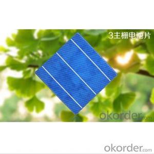
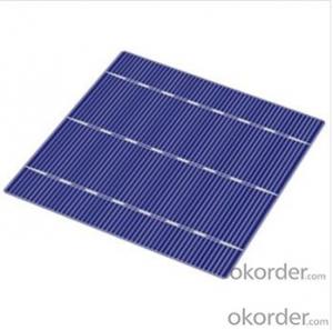
Monosolicion Solar Cells Poly 156mm*156mm
- Ref Price:
-

- Loading Port:
- China main port
- Payment Terms:
- TT OR LC
- Min Order Qty:
- 100 watt
- Supply Capability:
- 10000 watt/month
OKorder Service Pledge
Quality Product, Order Online Tracking, Timely Delivery
OKorder Financial Service
Credit Rating, Credit Services, Credit Purchasing
You Might Also Like


Monosolicion Solar Cells Poly 156mm*156mm
Typical electrical characteristics
Efficiency code | 1720 | 1740 | 1760 | 1780 | 1820 | 1840 | |
Efficiency (min) | (%) | 17.2 | 17.4 | 17.6 | 17.8 | 18.2 | 18.4 |
Pmax | (W) | 4.186 | 4.234 | 4.283 | 4.332 | 4.429 | 4.478 |
Voc | (V) | 0.631 | 0.632 | 0.634 | 0.636 | 0.640 | 0.642 |
Isc | (A) | 8.446 | 8.485 | 8.523 | 8.573 | 8.660 | 8.700 |
Vmp | (V) | 0.525 | 0.527 | 0.529 | 0.531 | 0.535 | 0.537 |
Imp | (A) | 7.973 | 8.035 | 8.097 | 8.160 | 8.280 | 8.340 |
Data under standard testing conditions(STC): 1,000W/m2, AM1.5, 25℃, Pmax: Positive power tolerance.
Typical teperature coefficients
Voltage | -2.08 | mV/K |
Current | +4.58 | mA/K |
Power | -0.40 | %/K |
Cell Picture


- Q:What is the role of back contacts on solar silicon wafers?
- The role of back contacts on solar silicon wafers is to provide an electrical connection between the silicon wafer and the external circuitry of the solar cell. They help in collecting the generated electricity from the front surface of the cell and ensure efficient transfer of the electrical current to the external load. Additionally, back contacts also help in providing structural support to the silicon wafer, allowing for easier handling and integration into the overall solar module.
- Q:Can solar silicon wafers be repaired?
- No, solar silicon wafers cannot be repaired once they are damaged.
- Q:Can solar silicon wafers be used in concentrated solar power (CSP) systems?
- Yes, solar silicon wafers can be used in concentrated solar power (CSP) systems. CSP systems use mirrors or lenses to concentrate sunlight onto a receiver, which then converts the solar energy into thermal or electrical energy. Silicon wafers can be used as the receiver material in CSP systems to efficiently capture and convert the concentrated sunlight into electricity.
- Q:What is the role of solar silicon wafers in reducing air pollution?
- Solar silicon wafers play a crucial role in reducing air pollution by serving as the key component in solar panels, which generate clean and renewable energy. By harnessing sunlight and converting it into electricity, solar panels powered by silicon wafers eliminate the need for fossil fuel-based power generation, thereby reducing harmful emissions that contribute to air pollution.
- Q:Why silicon wafers are made in watts! There are several specifications for silicon wafers!
- Crystalline silicon photovoltaic cells have two types of monocrystalline silicon and polycrystalline silicon, with P (or n) silicon substrate, through the formation of phosphorus (or boron) diffusion Pn formation, production technology is mature, is the leading product in the photovoltaic market. The buried layer electrode, surface passivation, enhanced light trapping, dense grid technology, optimization of back electrode and contact electrode technology, improve the collection efficiency of carrier materials, optimization of anti elbow membrane, concave convex surface, high reflective back electrode, the photoelectric conversion efficiency is greatly improved. Silicon photocell area is limited, the larger the phi 10 to 20cm wafer, the annual production capacity of 46MW/a. At present, the main task is to continue to expand the scale of the industry, the development of ribbon silicon photovoltaic technology, improve material utilization. Internationally recognized as the highest efficiency under AM1.5 conditions of 24%, the space with high quality efficiency in the AMO condition is about 13.5 - 18% of the ground with a large number of production in the AM1 conditions in the more than 11 - 18%. It can reduce the cost, but the efficiency is lower, which is made by the method of directional solidification. Optimization of the silver electrode and aluminum paste screen printing, grinding and polishing process, do everything possible to further reduce costs, improve efficiency, the maximum conversion efficiency of polycrystalline silicon photovoltaic cells up to 18.6%.
- Q:What is the average reflectivity of a solar silicon wafer?
- The average reflectivity of a solar silicon wafer is typically around 30%.
- Q:What is the role of oxide layers on solar silicon wafers?
- The role of oxide layers on solar silicon wafers is to passivate the surface and protect the underlying silicon material from impurities and defects. These oxide layers act as a barrier, preventing recombination of charge carriers and improving the efficiency of the solar cell by reducing surface recombination. Additionally, oxide layers can also provide an anti-reflective coating, helping to increase the amount of light absorbed by the solar cell.
- Q:What are the main factors that affect the lifespan of a solar silicon wafer?
- The main factors that affect the lifespan of a solar silicon wafer are material degradation, environmental conditions, and manufacturing defects. Material degradation refers to the gradual breakdown of the silicon material due to various factors such as heat, light exposure, and chemical reactions. Environmental conditions such as temperature, humidity, and exposure to harsh weather elements can also impact the wafer's lifespan. Additionally, manufacturing defects, such as impurities or flaws introduced during the fabrication process, can affect the wafer's performance and longevity.
- Q:Are there any advancements in solar silicon wafer surface texturing techniques?
- Yes, there have been advancements in solar silicon wafer surface texturing techniques. Researchers and engineers have been exploring various methods to enhance the efficiency of solar cells by improving the light absorption capacity of silicon wafers. Some recent advancements include laser texturing, chemical etching, and nano-imprinting techniques, which help create unique surface textures that increase the trapping and absorption of sunlight, leading to improved energy conversion. These advancements aim to maximize the performance of solar cells and contribute to the overall growth and adoption of solar energy technology.
- Q:How do solar silicon wafers perform in high humidity conditions?
- Solar silicon wafers generally perform well in high humidity conditions. However, excessive moisture can potentially affect their performance and efficiency by causing corrosion or oxidation of the surfaces. Therefore, it is important to ensure proper sealing and protection of the wafers to mitigate any negative impact of high humidity on their performance.
1. Manufacturer Overview |
|
|---|---|
| Location | |
| Year Established | |
| Annual Output Value | |
| Main Markets | |
| Company Certifications | |
2. Manufacturer Certificates |
|
|---|---|
| a) Certification Name | |
| Range | |
| Reference | |
| Validity Period | |
3. Manufacturer Capability |
|
|---|---|
| a)Trade Capacity | |
| Nearest Port | |
| Export Percentage | |
| No.of Employees in Trade Department | |
| Language Spoken: | |
| b)Factory Information | |
| Factory Size: | |
| No. of Production Lines | |
| Contract Manufacturing | |
| Product Price Range | |
Send your message to us
Monosolicion Solar Cells Poly 156mm*156mm
- Ref Price:
-
- Loading Port:
- China main port
- Payment Terms:
- TT OR LC
- Min Order Qty:
- 100 watt
- Supply Capability:
- 10000 watt/month
OKorder Service Pledge
Quality Product, Order Online Tracking, Timely Delivery
OKorder Financial Service
Credit Rating, Credit Services, Credit Purchasing
Similar products


New products
Hot products


Related keywords