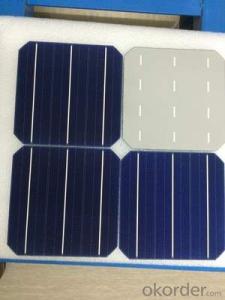
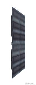
Mono Solar Cells156mm*156mm in Bulk Quantity Low Price Stock 20.0
- Ref Price:
-

- Loading Port:
- Shanghai
- Payment Terms:
- TT OR LC
- Min Order Qty:
- 1000 pc
- Supply Capability:
- 100000 pc/month
OKorder Service Pledge
OKorder Financial Service
You Might Also Like


Brief Introduction
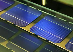
- Up to 20.0% efficiency, one of the highest performing mono crystalline cells on the market
- Three bus bars boosts current collection over the entire cell area, leading to higher fill factors
- Blue anti-reflecting coating allows more sunlight be captured and converted to electricity
- Finer, closer fingers improves charge collections for improved energy yield
- Lower light-induced degradation leads to greater power output over the entire module lifetime
- All solar cells are tightly classified to optimize output of module
- Maximum yield and longevity due to hotspot prevention
- Premium appearance results in a highly uniform and aesthetically appealing module
Specification
- Product Mono-crystalline silicon solar cell
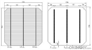
- Dimension 156 mm x 156 mm ± 0.5 mm
- Thickness 200 μm ± 30 μm
- Front 1.5 ± 0.1 mm busbar (silver)
- Silicon nitride antireflection coating
- Back 3.0 mm continuous soldering pads (silver)
- Back surface field (aluminum)
Electric performance parameters

- Testing conditions: 1000 W/m2, AM 1.5, 25 °C, Tolerance: Efficiency ± 0.2% abs., Pmpp ±1.5% rel.
- Imin : at 0.5 V
Light Intensity Dependence

Soldering Ability
- Peel Strength: > 1.0 N/mm (Pull soldered ribbon from busbar in 5 mm/s of 180°)
Dimension Figure

Quick Response
- Any time and anywhere, reply clients' email and solve all problems happen in the work at the first time.
- Remove clients doubts and offer the best solution at the first time.
- Give our clients the lastest news of the photovoltaic, update the newest stock informtion.
Production and Quality Control
- Precision cell efficiency sorting procedures
- Stringent criteria for color uniformity and appearance
- Reverse current and shunt resistance screening
- ISO9001,ISO14001 and OHSAS 18001,TUV Certificated


FAQ:
1. Q: Do you have your own factory?
A: Yes, we have. Our factory located in Jiangsu
2. Q: How can I visit your factory?
A: Before you visit,please contact us.We will show you the route or arrange a car to pick you up.
3. Q: Do you provide free sample?
A: Commenly we provide paid sample.
4. Q: Could you print our company LOGO on the nameplate and package?
A: Yes, we accept it.And need an Authorization Letter from you.
5. Q: Do you accept custom design on size?
A: Yes, if the size is reasonable.
6. Q: How can I be your agent in my country?
A: Please leave feedback. It's better for us to talk about details by email.
7. Q: Do you have solar project engineer who can guide me to install system?
A: Yes, we have a professional engineer team. They can teach you how to install a solar system.
- Q:What is the purpose of a spectral response in a solar silicon wafer?
- The purpose of a spectral response in a solar silicon wafer is to measure the efficiency of the wafer in converting different wavelengths of sunlight into electricity. By analyzing the spectral response, we can assess the performance of the silicon wafer under different light conditions and optimize its design for maximum energy conversion.
- Q:Can solar silicon wafers be used in solar-powered agricultural applications?
- Yes, solar silicon wafers can be used in solar-powered agricultural applications. These wafers are commonly used to manufacture solar panels, which can be utilized to power various agricultural applications such as irrigation systems, greenhouse ventilation, and livestock water pumps. The solar panels convert sunlight into electricity, providing a clean and renewable energy source for agricultural purposes.
- Q:How are solar silicon wafers protected from theft?
- Solar silicon wafers are typically protected from theft through various security measures. These may include surveillance cameras, alarm systems, secure storage facilities, and restricted access to the production areas. Additionally, tracking technologies like RFID tags or GPS can be used to monitor and locate stolen wafers. These measures aim to deter theft, detect any unauthorized activity, and enable quick recovery in case of theft.
- Q:How to detect the surface finish of photovoltaic silicon wafers, what equipment?
- Do you want to check the surface roughness or do you want to clean it? These two are not the same,
- Q:Why is it not easy to use high resistance on the silicon chip integrated circuit
- In some places, the resistance of the epitaxial layer is adopted, and the resistance is N type, which has a lot of inconvenience in the circuit, and the numerical value is also very difficult to do
- Q:Can solar silicon wafers be used in disaster response vehicles?
- Yes, solar silicon wafers can be used in disaster response vehicles. Solar panels equipped with silicon wafers can generate electricity from sunlight, providing a sustainable and renewable power source for various functions in disaster response vehicles, including lighting, communication systems, and charging equipment. This helps reduce reliance on traditional fuel sources and ensures continuous power supply even in remote or disrupted areas during disaster response operations.
- Q:Are solar silicon wafers susceptible to cracking?
- Yes, solar silicon wafers are susceptible to cracking.
- Q:How are solar silicon wafers affected by light trapping techniques?
- Solar silicon wafers are positively influenced by light trapping techniques as these methods improve the absorption of light within the wafer, thereby enhancing its overall efficiency in converting sunlight into electricity. Light trapping techniques, such as texturing the surface or adding anti-reflective coatings, help to increase the path length of light within the wafer, ensuring that more photons are absorbed and utilized. This results in higher power output and improved performance of solar cells using silicon wafers.
- Q:What are the reasons for the emergence of the black chip phenomenon of the monocrystalline silicon, which aspects of the production process have an impact on it, preventive measures, and improvement measures?
- Preventive measures are in the ultra clean environment, indirect or direct contact with the silicon process, can not have any metal objects, especially stainless steel, is determined not to appear. There's a silicon chip! It is necessary to ensure the cleanliness of the chemical cleaning liquid, and the ratio is correct. Otherwise, it will also appear on the surface of the silicon wafer. Check polishing machine polishing head, calibration pressure. Also, there can not be bad to the silicon wafer, belonging to scrap wafers, shall be returned to the original factory to find the reasons.
- Q:What are the main defects in solar silicon wafers?
- The main defects in solar silicon wafers can include impurities, such as iron or boron, which can reduce the efficiency of the solar cells. Other defects may include cracks, dislocations, or grain boundaries, which can affect the structural integrity and electrical performance of the wafers.
1. Manufacturer Overview |
|
|---|---|
| Location | |
| Year Established | |
| Annual Output Value | |
| Main Markets | |
| Company Certifications | |
2. Manufacturer Certificates |
|
|---|---|
| a) Certification Name | |
| Range | |
| Reference | |
| Validity Period | |
3. Manufacturer Capability |
|
|---|---|
| a)Trade Capacity | |
| Nearest Port | |
| Export Percentage | |
| No.of Employees in Trade Department | |
| Language Spoken: | |
| b)Factory Information | |
| Factory Size: | |
| No. of Production Lines | |
| Contract Manufacturing | |
| Product Price Range | |
Send your message to us
Mono Solar Cells156mm*156mm in Bulk Quantity Low Price Stock 20.0
- Ref Price:
-
- Loading Port:
- Shanghai
- Payment Terms:
- TT OR LC
- Min Order Qty:
- 1000 pc
- Supply Capability:
- 100000 pc/month
OKorder Service Pledge
OKorder Financial Service
Similar products


New products
Hot products


Hot Searches
Related keywords