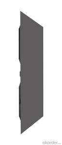
Mono Solar Cells156mm*156mm in Bulk Quantity Low Price Stock 19.0
- Ref Price:
-

- Loading Port:
- Shanghai
- Payment Terms:
- TT OR LC
- Min Order Qty:
- 1000 pc
- Supply Capability:
- 100000 pc/month
OKorder Service Pledge
OKorder Financial Service
You Might Also Like


Brief Introduction
- Up to 20.0% efficiency, one of the highest performing mono crystalline cells on the market
- Three bus bars boosts current collection over the entire cell area, leading to higher fill factors
- Blue anti-reflecting coating allows more sunlight be captured and converted to electricity
- Finer, closer fingers improves charge collections for improved energy yield
- Lower light-induced degradation leads to greater power output over the entire module lifetime
- All solar cells are tightly classified to optimize output of module
- Maximum yield and longevity due to hotspot prevention
- Premium appearance results in a highly uniform and aesthetically appealing module
Specification
- Product Mono-crystalline silicon solar cell
- Dimension 156 mm x 156 mm ± 0.5 mm
- Thickness 200 μm ± 30 μm
- Front 1.5 ± 0.1 mm busbar (silver)
- Silicon nitride antireflection coating
- Back 3.0 mm continuous soldering pads (silver)
- Back surface field (aluminum)
Electric performance parameters

- Testing conditions: 1000 W/m2, AM 1.5, 25 °C, Tolerance: Efficiency ± 0.2% abs., Pmpp ±1.5% rel.
- Imin : at 0.5 V
Light Intensity Dependence

Soldering Ability
- Peel Strength: > 1.0 N/mm (Pull soldered ribbon from busbar in 5 mm/s of 180°)
Dimension Figure

Quick Response
- Any time and anywhere, reply clients' email and solve all problems happen in the work at the first time.
- Remove clients doubts and offer the best solution at the first time.
- Give our clients the lastest news of the photovoltaic, update the newest stock informtion.
Production and Quality Control
- Precision cell efficiency sorting procedures
- Stringent criteria for color uniformity and appearance
- Reverse current and shunt resistance screening
- ISO9001,ISO14001 and OHSAS 18001,TUV Certificated


FAQ:
1. Q: Do you have your own factory?
A: Yes, we have. Our factory located in Jiangsu
2. Q: How can I visit your factory?
A: Before you visit,please contact us.We will show you the route or arrange a car to pick you up.
3. Q: Do you provide free sample?
A: Commenly we provide paid sample.
4. Q: Could you print our company LOGO on the nameplate and package?
A: Yes, we accept it.And need an Authorization Letter from you.
5. Q: Do you accept custom design on size?
A: Yes, if the size is reasonable.
6. Q: How can I be your agent in my country?
A: Please leave feedback. It's better for us to talk about details by email.
7. Q: Do you have solar project engineer who can guide me to install system?
A: Yes, we have a professional engineer team. They can teach you how to install a solar system.
- Q:I would like to ask the solar cell (silicon) production process is the principle of how
- Solar cell production processThe production process of solar cell can be divided into three parts: silicon wafer testing, surface texturing, diffusion bonding, phosphorus removal, silica glass, plasma etching, antireflection coating, screen printing, rapid sintering and so on. Details are as follows:
- Q:What are the impurities in a solar silicon wafer?
- The impurities in a solar silicon wafer mainly include elements such as boron, phosphorus, and oxygen. These impurities can affect the electrical properties of the silicon, and their precise concentration and distribution are crucial for optimizing the efficiency and performance of solar cells.
- Q:What is the role of a solar silicon wafer in a solar panel?
- The role of a solar silicon wafer in a solar panel is to capture and convert sunlight into electricity. The wafer acts as the semiconductor material that absorbs the photons from the sunlight and generates an electric current through the photovoltaic effect. It is a crucial component in a solar panel as it directly converts solar energy into usable electrical energy.
- Q:Polished silicon wafers can be most SEM substrates
- In other words, only nano materials will consider the use of polished silicon wafer sample carrier. Micron submicron level, waste, direct double-sided conductive adhesive tape can be.
- Q:What is the impact of crystal orientation on solar silicon wafers?
- The crystal orientation of silicon wafers used in solar cells has a significant impact on their efficiency and performance. The orientation determines how well the wafer can absorb and convert sunlight into electricity. Silicon wafers with specific crystal orientations, such as (100), (110), or (111), exhibit different electrical and optical properties. For instance, (100) oriented wafers have higher carrier mobility, which enhances charge transport and reduces recombination, resulting in improved efficiency. On the other hand, (111) oriented wafers have a lower defect density and higher surface passivation qualities, leading to better light trapping and higher open-circuit voltages. Therefore, the crystal orientation of solar silicon wafers plays a crucial role in determining their overall performance and efficiency in converting sunlight into usable electricity.
- Q:How to make monocrystalline silicon solar panels? Begged: specific steps
- Wafer inspectionSilicon wafer is the carrier of solar cell, the quality of silicon wafer directly determines the conversion efficiency of solar cell. This procedure is mainly used to measure the technical parameters of silicon wafer on line. These parameters mainly include the surface roughness of the silicon wafer, the lifetime of the minority, the resistivity, the P/N type and the micro crack. The device is divided into four parts: automatic loading and unloading, silicon wafer transmission, system integration part and. The silicon photovoltaic detector on the silicon wafer surface roughness were detected, and the size and appearance of diagonal parameter detection chip; micro crack detection module is used to detect silicon micro cracks; another two detecting module, a [url=] module [/url] online test mainly test wafer resistivity and wafer type, on the other a module for lifetime test wafer. The detection of the diagonal and micro cracks of the silicon wafer is needed before the sub lifetime and resistivity measurement. Wafer inspection equipment can automatic loading and unloading, and substandard products in a fixed position, so as to improve the detection accuracy and efficiency.
- Q:How do solar silicon wafers perform in coastal areas?
- Solar silicon wafers generally perform well in coastal areas as long as they are properly protected against the corrosive effects of saltwater and strong winds.
- Q:How are solar silicon wafers protected from transportation damage?
- Solar silicon wafers are protected from transportation damage through the use of specialized packaging materials and handling procedures. These wafers are typically placed in anti-static trays or boxes, which provide cushioning and prevent physical impact during transit. Additionally, shock-absorbing materials such as foam or bubble wrap may be used to further protect the wafers from vibrations or jolts. Furthermore, stringent quality control measures are implemented to ensure that the packaging is secure and that the wafers are not exposed to extreme temperatures or humidity, which could potentially damage their delicate structure.
- Q:What is the purpose of surface texturing in solar silicon wafers?
- The purpose of surface texturing in solar silicon wafers is to increase the light absorption capability of the wafer by creating microstructures on its surface. These microstructures help to trap and scatter light, allowing for more efficient capture of sunlight and conversion into electricity.
- Q:How do solar silicon wafers contribute to reducing carbon emissions?
- Solar silicon wafers contribute to reducing carbon emissions by serving as the building blocks for solar cells, which convert sunlight into electricity. By harnessing renewable solar energy rather than relying on fossil fuels, solar silicon wafers enable the generation of clean and emissions-free electricity. This helps to reduce the reliance on carbon-intensive power sources, such as coal or natural gas, thus significantly decreasing carbon emissions and mitigating climate change.
1. Manufacturer Overview |
|
|---|---|
| Location | |
| Year Established | |
| Annual Output Value | |
| Main Markets | |
| Company Certifications | |
2. Manufacturer Certificates |
|
|---|---|
| a) Certification Name | |
| Range | |
| Reference | |
| Validity Period | |
3. Manufacturer Capability |
|
|---|---|
| a)Trade Capacity | |
| Nearest Port | |
| Export Percentage | |
| No.of Employees in Trade Department | |
| Language Spoken: | |
| b)Factory Information | |
| Factory Size: | |
| No. of Production Lines | |
| Contract Manufacturing | |
| Product Price Range | |
Send your message to us
Mono Solar Cells156mm*156mm in Bulk Quantity Low Price Stock 19.0
- Ref Price:
-
- Loading Port:
- Shanghai
- Payment Terms:
- TT OR LC
- Min Order Qty:
- 1000 pc
- Supply Capability:
- 100000 pc/month
OKorder Service Pledge
OKorder Financial Service
Similar products


New products


Hot products


Hot Searches
Related keywords